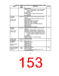
Table 64 - Auxiliary I/O, Logical Device 8 [Logical Device Number = 0x08]
NAME
REG
DEFINITION
STATE
INDEX
Bit[3] Reserved
Bit[4] EN_P12: Enable 8042 P1.2 to route internally
to nSMI. 0=Do not route to nSMI, 1=Enable
routing to nSMI.
Bit[5] Reserved
Bit[6] EN_SMI_S: Enables nSMI Interrupt onto
Serial IRQ.
Bit[7] Reserved
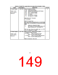
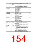
SMI Status
Register 1
0xB6 R/W
This register is used to read the status of the SMI
inputs.
C
The following bits must be cleared at their source.
Bit[0] Reserved
Default = 0x00
on Vcc POR
Bit[1] PINT (Parallel Port Interrupt)
Bit[2] U2INT (UART 2 Interrupt)
Bit[3] U1INT (UART 1 Interrupt)
Bit[4] FINT (Floppy Disk Controller Interrupt)
Bit[5] Reserved
Bit[6] Reserved
Bit[7] WDT (Watch Dog Timer)
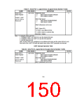
This register is used to read the status of the SMI
inputs.
SMI Status
Register 2
0xB7 R/W
C
Bit[0] MINT: Mouse Interrupt. Cleared at source.
Bit[1] KINT: Keyboard Interrupt. Cleared at source.
Bit[2] IRINT: This bit is set by a transition on the IR
pin (RDX2 or IRRX as selected in CR L5-F1-B6
i.e., after the MUX). Cleared by a read of this
register.
Default = 0x00
on Vcc POR
Bit[3] Reserved
Bit[4] P12: 8042 P1.2. Cleared at source
Bit[7:5] Reserved
Default = 0x00
on VTR POR
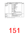
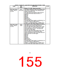
Pin Multiplex
Controls
0xB8 R/W
0xC0
Bits[7:0] Reserved
C
Bit[0] Reserved
Bit[1] DMA 3 Select
Bit[2] Reserved
Default = 0x02 on
Vcc POR
Bit[3] 8042 Select
Bit[4] Reserved
Bit[5:7] Reserved
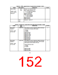
Force Disk Change
Default = 0x03 on
Vcc POR
0xC1
(R/W)
Bit[0] Force Change 0
Bit[7:1] Reserved
Force Change[0] can be written to 1 but is not
clearable by software.
C,R
153

 SMSC [ SMSC CORPORATION ]