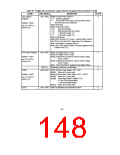
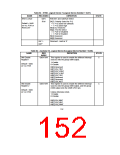
Table 63 - KYBD, Logical Device 7 [Logical Device Number = 0x07]
NAME
REG INDEX
0xF0
DEFINITION
KRESET and GateA20 Select
STATE
KRST_GA20
R/W
Bit[7] Polarity Select for P12
= 0 P12 active low (default)
= 1 P12 active high
Bits[6:3] Reserved
Default = 0x00
on Vcc POR or
Reset_Drv
Bit[2] Port 92 Select
= 0 Port 92 Disabled
= 1 Port 92 Enabled
Bit[1] Reserved
Bit[0] Reserved
0xF1 -
0xFF
Reserved - read as ‘0’
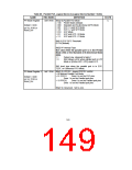
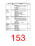
Table 64 - Auxiliary I/O, Logical Device 8 [Logical Device Number = 0x08]
NAME
REG
INDEX
DEFINITION
STATE
SMI Enable
Register 1
0xB4 R/W
This register is used to enable the different interrupt
sources onto the group nSMI output.
C
1=Enable
0=Disable
Default = 0x00
on Vcc POR
Bit[0] Reserved
Bit[1] EN_PINT
Bit[2] EN_U2INT
Bit[3] EN_U1INT
Bit[4] EN_FINT
Bit[5] Reserved
Bit[6] Reserved
Bit[7] EN_WDT
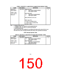
SMI Enable
Register 2
0xB5 R/W
This register is used to enable the different interrupt
sources onto the group nSMI output, and the group
nSMI output onto the nSMI GPI/O pin.
C
Default = 0x00
on Vcc POR
Unless otherwise noted,
1=Enable
0=Disable
Bit[0] EN_MINT
Bit[1] EN_KINT
Bit[2] EN_IRINT
152

 SMSC [ SMSC CORPORATION ]