5Mbps ARCNET (ANSI 878.1) Controller with 2K x 8 On-Chip RAM
Datasheet
Chapter 7 Operational Description
7.1
Maximum Guaranteed Ratings*
Operating Temperature Range ..................................................................................................0oC to +70oC
Storage Temperature Range ................................................................................................-55oC to +150oC
Lead Temperature (soldering, 10 seconds) ....................................................................................... +325 oC
Positive Voltage on any pin, with respect to ground ........................................................................VDD+0.3V
Negative Voltage on any pin, with respect to ground............................................................................. -0.3V
Maximum VDD .......................................................................................................................................... +7V
* Stresses above those listed may cause permanent damage to the device. This is a stress rating only and
functional operation of the device at these or any other condition above those indicated in the operational
sections of this specification is not implied.
Note:
When powering this device from laboratory or system power supplies, it is important that the Absolute
Maximum Ratings not be exceeded or device failure can result. Some power supplies exhibit voltage
spikes or "glitches" on their outputs when the AC power is switched on or off. In addition, voltage
transients on the AC power line may appear on the DC output. If this possibility exists it is suggested that
a clamp circuit be used.
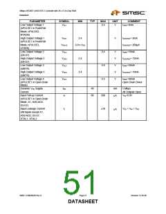
7.2
DC Electrical Characteristics
VDD=5.0V±10%
COM20020: TA=0oC to +70oC, COM20020I: TA=-40oC to +85oC
PARAMETER
SYMBOL
MIN
TYP
MAX
UNIT
COMMENT
TTL Levels
Low Input Voltage 1
(All inputs except A2,
XTAL1, nRESET, nRD,
nWR, and RXIN)
High Input Voltage 1
(All inputs except A2,
XTAL1, nRESET, nRD,
nWR, and RXIN)
Low Input Voltage 2
(XTAL1)
VIL1
0.8
V
VIH1
2.0
V
TTL Levels
VIL2
VIH2
VILH
1.0
V
V
V
TTL Clock Input
High Input Voltage 2
(XTAL1)
4.0
Low to High Threshold
Input Voltage
1.8
1.2
Schmitt Trigger,
All Values at VDD
5V
=
(A2, nRESET, nRD, nWR, and
RXIN)
High to Low Threshold
Input Voltage
VIHL
V
(A2, nRESET, nRD, nWR, and
RXIN)
Revision 12-05-06
Page 50
SMSC COM20020I Rev D
DATASHEET

 SMSC [ SMSC CORPORATION ]