Legacy-Free Keyboard/Embedded Controller with SPI and LPC Docking Interface
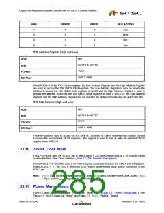
NSH
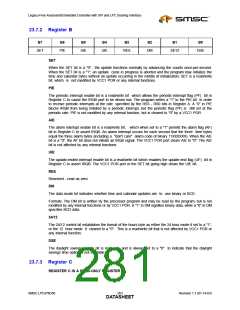
KREQX
HREQX
BUS ACCESS
1
0
0
0
X
0
1
0
X
0
0
1
Host
None
8051
Host
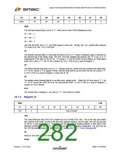
RTC Address Register (High and Low)
N/A
HOST
0x7FF8 & 0x7FF6
VCC1
8051
POWER
DEFAULT
0x00 & 0x00
When KREQ=1 in the RTC Control register, the Low Address Register and the High Address Register
are used to access the 256 CMOS RAM registers. The Low Address Register is used to provide the
address to access the 128 CMOS RAM registers in bank0 and the High Address Register is used to
provide the address to access the 128 CMOS RAM registers in bank1. Bit D7 of the Low Address
Register and the High Address Register are not used for the address decode and are don’t care bits.
RTC Data Register (High and Low)
N/A
HOST
0x7FF9 & 0x7FF7
VCC1
8051
POWER
DEFAULT
0x00 & 0x00
The low register is used to access the first bank of 128 bytes, in CMOS RAM the high register is used
to access the second bank of 128 registers. This register is used to read or write the selected CMOS
register when KREQ=1.
23.10 32kHz Clock Input
The LPC47N350 uses the XOSEL pin to select either a 32.768kHz input clock or a 32.768kHz crystal
to drive the Real Time Clock Interface (Table 2.2, "Pin Function Description").
When XOSEL = ‘0’, the RTC uses a 32.768kHz crystal connected between the XTAL1 and XTAL2 pins.
When XOSEL = ‘1’, the RTC is driven by a 32.768kHz single-ended clock source connected to the
XTAL2 pin.
Note:
I
≥ 10µA for time-keeping operations under V
using a single-ended clock source. I
CC0 CC1
CC0
= 30µA under V
using a single-ended clock source.
CC1
23.11 Power Management
The RTC and CMOS RAM utilize VCC0 power plane (see Section 2.3, "Power Configuration"). See
Figure 2.2, "VCC2 Power-Up Timing" and Figure 2.3, "VCC1_PWRGD Timing".
SMSC LPC47N350
267
Revision 1.1 (01-14-03)
DATASHEET

 SMSC [ SMSC CORPORATION ]