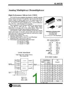
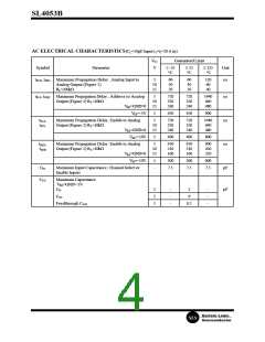
SL4053B
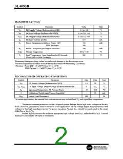
MAXIMUM RATINGS*
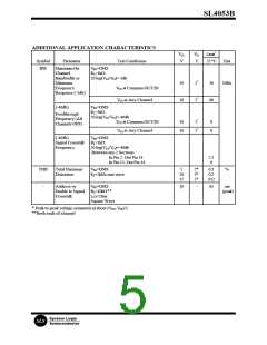
Symbol
Parameter
Value
-0.5 to +20
-0.5 to VCC +0.5
-0.5 to VCC +0.5
±10
Unit
V
VCC
DC Supply Voltage (Referenced to GND)
DC Input Voltage (Referenced to GND)
DC Output Voltage (Referenced to GND)
DC Input Current, per Pin
V
IN
V
VOUT
IIN
V
mA
mW
PD
Power Dissipation in Still Air, Plastic DIP+
SOIC Package+
750
500
PD
Tstg
TL
Power Dissipation per Output Transistor
Storage Temperature
100
-65 to +150
260
mW
°C
Lead Temperature, 1 mm from Case for 10 Seconds
(Plastic DIP or SOIC Package)
°C
*Maximum Ratings are those values beyond which damage to the device may occur.
Functional operation should be restricted to the Recommended Operating Conditions.
+Derating - Plastic DIP: - 10 mW/°C from 65° to 125°C
SOIC Package: : - 7 mW/°C from 65° to 125°C
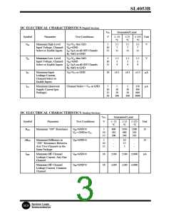
RECOMMENDED OPERATING CONDITIONS
Symbol
VCC
Parameter
Min
3.0
0
Max
18
Unit
DC Supply Voltage (Referenced to GND)
DC Input Voltage, Output Voltage (Referenced to GND)
Operating Temperature, All Package Types
Multiplexer Switch Input Current Capability*
Output Load Resistance
V
V
V , VOUT
IN
VCC
+125
25
TA
I
-55
-
°C
mA
W
ROH
100
-
* In certain applications, the external load-resistor current may include both VCC and signal-line components.
This device contains protection circuitry to guard against damage due to high static voltages or electric
fields. However, precautions must be taken to avoid applications of any voltage higher than maximum rated
voltages to this high-impedance circuit. For proper operation, V and VOUT should be constrained to the range
IN
GND£(V or VOUT)£VCC.
IN
Unused digital pins must be tied to an appropriate logic voltage level (e.g., either GND or V ). Unused
CC
Analog I/O pins may be left open or terminated.
System Logic
SLS

 SLS [ SYSTEM LOGIC SEMICONDUCTOR ]