SL74HC573
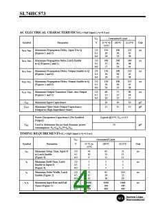
AC ELECTRICAL CHARACTERISTICS(CL=50pF,Input tr=tf=6.0 ns)
VCC
Guaranteed Limit
Symbol
Parameter
V
25 °C to £85°C
-55°C
£125°C
Unit
ns
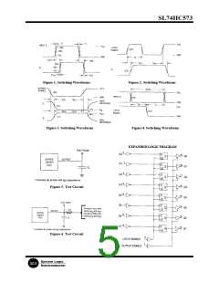
tPLH, tPHL Maximum Propagation Delay, Input D to Q
(Figures 1 and 5)
2.0
4.5
6.0
150
30
190
38
225
45
38
26
33
tPLH, tPHL Maximum Propagation Delay,Latch Enable
to Q (Figures 2 and 5)
2.0
4.5
6.0
160
32
27
200
40
34
240
48
41
ns
ns
ns
ns
tPLZ, tPHZ Maximum Propagation Delay, Output Enable to Q
(Figures 3 and 6)
2.0
4.5
6.0
150
30
26
190
38
33
225
45
38
tPZH, tPZL Maximum Propagation Delay, Output Enable to Q
(Figures 3 and 6)
2.0
4.5
6.0
150
30
26
190
38
33
225
45
38
tTLH, tTHL Maximum Output Transition Time, Any Output
(Figures 1 and 5)
2.0
4.5
6.0
60
12
10
75
15
13
90
18
15
CIN
Maximum Input Capacitance
-
-
10
15
10
15
10
15
pF
pF
COUT
Maximum Three-State Output Capacitance
(Output in High-Impedance State)
Power Dissipation Capacitance (Per Enabled
Output)
Typical @25°C,VCC=5.0 V
CPD
Used to determine the no-load dynamic power
consumption: PD=CPDVCC2f+ICCVCC
23
pF
TIMING REQUIREMENTS (CL=50pF,Input tr=tf=6.0 ns)
VCC
Guaranteed Limit
Symbol
tSU
Parameter
V
25 °C to
-55°C
£85°C
£125°C
Unit
Minimum Setup Time, Input D
to Latch Enable
2.0
4.5
6.0
50
10
9
65
13
11
75
15
13
ns
ns
ns
ns
(Figure 4)
th
Minimum Hold Time, Latch
Enable to Input D
(Figure 4)
2.0
4.5
6.0
5
5
5
5
5
5
5
5
5
tw
Minimum Pulse Width, Latch
Enable (Figure 2)
2.0
4.5
6.0
75
15
13
95
19
16
110
22
19
tr, tf
Maximum Input Rise and Fall
Times (Figure 1)
2.0
4.5
6.0
1000
500
400
1000
500
400
1000
500
400
System Logic
SLS

 SLS [ SYSTEM LOGIC SEMICONDUCTOR ]