SL74HC174
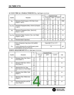
AC ELECTRICAL CHARACTERISTICS(CL=50pF,Input tr=tf=6.0 ns)
VCC
Guaranteed Limit
Symbol
fmax
Parameter
V
25 °C to £85°C
-55°C
£125°C
Unit
Maximum Clock Frequency (50% Duty Cycle)
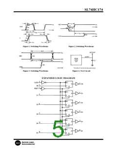
(Figures 1 and 4)
2.0
4.5
6.0
6.0
30
35
4.8
24
28
4.0
20
24
MHz
tPLH, tPHL Maximum Propagation Delay, Clock to Q (Figures
1 and 4)
2.0
4.5
6.0
110
22
19
140
28
24
165
33
28
ns
ns
ns
pF
tPHL
Maximum Propagation Delay , Reset to Q
(Figures 2 and 4)
2.0
4.5
6.0
110
21
19
140
28
24
160
32
27
tTLH, tTHL Maximum Output Transition Time, Any Output
(Figures 1 and 4)
2.0
4.5
6.0
75
15
13
95
19
16
110
22
19
CIN
Maximum Input Capacitance
-
10
10
10
Power Dissipation Capacitance (Per Enabled
Output)
Typical @25°C,VCC=5.0 V
CPD
Used to determine the no-load dynamic power
consumption: PD=CPDVCC2f+ICCVCC
62
pF
TIMING REQUIREMENTS (CL=50pF,Input tr=tf=6.0 ns)
VCC
Guaranteed Limit
Symbol
tSU
Parameter
V
25 °C to
-55°C
£85°C
£125°C
Unit
Minimum Setup Time, Data to
Clock (Figure 3)
2.0
4.5
6.0
50
10
9
65
13
11
75
15
13
ns
ns
ns
ns
ns
ns
th
trec
tw
Minimum Hold Time, Clock to
Data (Figure 3)
2.0
4.5
6.0
5
5
5
5
5
5
5
5
5
Minimum Recovery Time,
Reset Inactive to Clock (Figure
2)
2.0
4.5
6.0
5
5
5
5
5
5
5
5
5
Minimum Pulse Width, Clock
(Figure 1)
2.0
4.5
6.0
75
15
13
95
19
16
110
22
19
tw
Minimum Pulse Width, Reset
(Figure 2)
2.0
4.5
6.0
75
15
13
95
19
16
110
22
19
tr, tf
Maximum Input Rise and Fall
Times (Figure 1)
2.0
4.5
6.0
1000
500
400
1000
500
400
1000
500
400
System Logic
Semiconductor
SLS

 SLS [ SYSTEM LOGIC SEMICONDUCTOR ]