ST7781
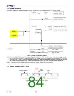
17.4. Voltage Generation
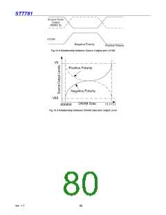
The pattern diagram for setting the voltages and the waveforms of the voltages of the ST7781 are as follows.
BT[2:0]
AVDD
VGH (10~16.5)V
VCI1
AVDD (4.5~5.6)V
VRH[3:0]
AVDD
GVDD
GVDD(3~(AVDD-0.5))V
VCOMH(3~(AVDD-0.5))V
VCOM[5:0]
VDV [4:0]
VDDI
VDD
VCOML((VCL+0.5)~0.0)V
VCI1
VCL
VCL=-VCI1
BT[2:0]
VGL(-14~-5)V
Fig.17.4 Voltage Configuration Diagram
Note1: The AVDD, VGH, VGL, and VCL output voltage levels are lower than their theoretical levels (ideal voltage levels)
due to current consumption at respective outputs. The voltage levels in the following relationships (AVDD – GVDD )
>0.5V, (VCOML – VCL) > 0.5V, are the actual voltage levels. When the alternating cycles of VCOM are set high (e.g.
the polarity inverts every line cycle), current consumption is large. In this case, check the voltage before use.
Note 2: In operation, setting voltages within the respective voltage ranges are recommended.
17.5. Applied Voltage to the TFT panel
Fig.17.5 Voltage Output to TFT LCD Panel
Ver. 1.7
84

 SITRONIX [ SITRONIX TECHNOLOGY CO., LTD. ]