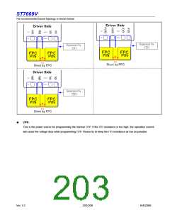
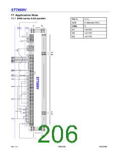
ST7669V
16 ITO /FPC Layout Guide
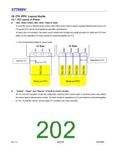
16.1 ITO Layout of Power
ꢁ
VDD, VDD2~VDD5, VSS, VSS1, VSS2 & VSS4:
To avoid the noise in different power system affect other power system, please separate different power source on
ITO layout (VDD can be short together to get better performance).
To reduce the ITO resistance, the power source should have enough trace width (includes ITO width and FPC trace
width). So the separated ITO traces should be connected together by FPC.
=> The recommended solution is shown below.
ICꢀSide
Separated by ITO
Short by ITO
ShortꢂonꢂFPC
ꢁ
“Output”, “Input” and “Sensor” of built-in power circuits:
The V0, XV0 and Vg power circuits have output pins, input pins and a sensor input. To avoid the power noise affects
the sensor input of internal power circuits. The trace should be separated by ITO and should be connected together
by FPC. So that the “Sensor” pin has larger ITO resistance (for noise immunity).
Ver 1.3
202/208
6/4/2008

 SITRONIX [ SITRONIX TECHNOLOGY CO., LTD. ]