ST7628
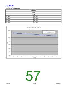
V0 fine tuning
ST7628 has 2 commands for fine tuning V0. These commands are VopOfsetInc (see section 9.1.48) and
VopOfsetDec (see section 9.1.49). When writing VopOfsetInc into IC for each time, V0 would increase 40mV; when writing
VopOfsetDec into IC for each time, V0 would decrease 40mV.
Example:
Vop[8:0]=011010010
Vopoffset[8:0]=000000011
EV[6:0]=0111111
VopOfsetInc x2
→ V0=3.6 +( 210 +3+ (63-63) +2 } x 0.04 =12.2 (V)
7.9.2 Voltage Follower Circuits
There is a built-in voltage follower circuits in ST7628 for generating Vg and Vm. These voltages are decided by bias ratio
selection circuitry which is set by users with software to control 1/5 to 1/12 bias ratios to match the optimum display
performance of LCD panel. Bias driving rule is listed below:
LCD bias
1/N bias
Vg
Vm
(2/N) x V0
(1/N) x V0
N=5 to 12
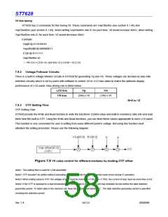
7.9.3 OTP Setting Flow
OTP Setting Flow
ST7628 provide the Write and Read function to write the Electronic Control value and Built-in resistance ratio into and read
them from the built-in OTP. Using the Write and Read functions, you can store these values appropriate to each LCD panel.
This function is very convenient for user in setting from some different panel’s voltage. But using this function must
attention the setting procedure. Please see the following diagram.
Figure 7.9 V0 value control for different modules by loading OTP offset
Note1: This setting flow is used for LCM assembler.
Note2: OTP shouldn’t be written without preceding loading correctly from OTP to avoid some errors during IC operation.
Note3: When writing value to OTP, the voltage of VPP must be more than 7.5V(7.5V~7.75V); the current of Ivpp must be more than 4 mA.
Note4: If the OTP is exposed to a high temperature for hours, data in the memory cell may probably be lost before the data retention
guarantee period. To retain data in the memory cell, keep the memory cell below 90
℃
. The data retention guarantee period is specified
including the retention period.
Ver 1.4
58/213
2008/08

 SITRONIX [ SITRONIX TECHNOLOGY CO., LTD. ]