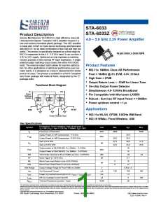
STA-6033 4.9-5.9 GHz Power Amp
Pin Out Description
Pin #
Function
Description
1,4,9,12,13
N/C
Pins are not used. May be grounded, left open, or connected to adjacent pin.
VPC1 is the bias control pin for the stage 1 active bias circuit. An external series resistor is required for
proper setting of bias levels. Refer to the evaluation board schematic for resistor value.
To prevent potential damage, do not apply voltage to this pin that is +1V greater than voltage applied to
pin 16 (Vbias) unless Vpc supply current capability is less than 10 mA.
5
6
7
VPC1
VPC2
VPC3
VPC2 is the bias control pin for the stage 2 active bias circuit. An external series resistor is required for
proper setting of bias levels. Refer to the evaluation board schematic for resistor value.
To prevent potential damage, do not apply voltage to this pin that is +1V greater than voltage applied to
pin 16 (Vbias) unless Vpc supply current capability is less than 10 mA.
VPC3 is the control pin for the stage 3 active bias circuits. An external series resistor is required for
proper setting of bias levels. Refer to the evaluation board schematic for resistor value.
To prevent potential damage, do not apply voltage to this pin that is +1V greater than voltage applied to
pin 16 (Vbias) unless Vpc supply current capability is less than 10 mA.
8
Vdet
Ouput power detector voltage. Load with 10K-100K ohms to ground for best performance.
RF input pins. This is DC grounded internal to the IC. Do not apply voltage to this pin. All three pins must
be used for proper operation.
2,3
RFIN
10,11
14
RFOUT RF output pin. This is also another connection to the 3rd stage collector
VC3
VC2
3rd stage collector bias pin. Apply 3.0V to 3.6V to this pin.
2nd stage collector bias pin. Apply 3.0V to 3.6V to this pin.
15
16
VC1,Vbias 1st stage collector bias pin and active bias network VCC. Apply 3.0V to 3.6V to this pin.
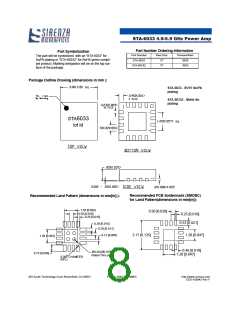
Exposed area on the bottom side of the package needs to be soldered to the ground plane of the board
for optimum thermal and RF performance. Several vias should be located under the EPAD as shown in
the recommended land pattern (page 5).
EPAD
Gnd
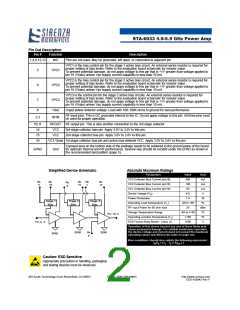
Simplified Device Schematic
Absolute Maximum Ratings
Parameters
Value
400
Unit
mA
mA
mA
V
VC3 Collector Bias Current (pin16)
VC2 Collector Bias Current (pin18)
VC1 Collector Bias Current (pin19)
Pin
5
Pin
16
Pin
15
Pin
7
Pin
14
Pin
6
140
50
Device Voltage (V )
D
4.5
Power Dissipation
1.4
W
Stage 1
Bias
Stage 2
Bias
Stage 3
Bias
Operating Lead Temperature (T )
L
-40 to +85
20
ºC
RF Input Power for 50 ohm load
Storage Temperature Range
dBm
ºC
-40 to +150
+150
1000
Pin 10,11
Operating Junction Temperature (T )
J
ºC
ESD Human Body Model - Class 1C
V
Pin 2, 3
Operation of this device beyond any one of these limits may
cause permanent damage. For reliable continuous operation
the device voltage and current must not exceed the maximum
operating values specified in the table on page one.
EPAD
Pin
8
EPAD
EPAD
Bias conditions should also satisfy the following expression:
I V < (T - T ) / R
j-l
D
D
J
L
TH’
Caution: ESD Sensitive
Appropriate precaution in handling, packaging
and testing devices must be observed.
303 South Technology Court Broomfield, CO 80021
Phone: (800) SMI-MMIC
2
http://www.sirenza.com
EDS-103643 Rev F

 SIRENZA [ SIRENZA MICRODEVICES ]