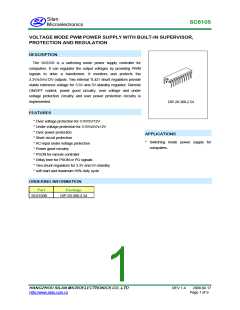
SC6105
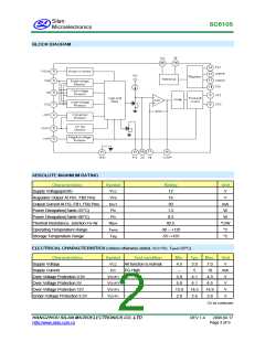
BLOCK DIAGRAM
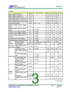
ABSOLUTE MAXIMUM RATING
Characteristics
Symbol
Rating
12
Unit
V
Supply Voltage(pin20)
V
CC
Regulator Output At FB1, FB2 Pins
Output Current At PG, FB1, FB2 Pins
Power Dissipation(Tamb=25°C)
Power Dissipation(Tamb=90°C)
Thermal Resistance, Junction•To•Air
Operating Temperature Range
Storage Temperature Range
V
16
V
FB
I
30
mA
W
OUT
P
P
1.5
D
0.5
W
D
RșJA
82.5
°C/W
°C
T
amb
•30 ~ +125
•55~+155
T
stg
°C
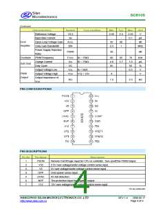
ELECTRICAL CHARACTERISTICS (Unless otherwise stated, V =5V, T
=25°C)
amb
CC
Characteristics
Supply Voltage
Symbol
Test condition
Min.
Typ.
5.0
5
Max.
Unit
V
V
CC
All function is normal.
4.5
••
7.0
10
Supply Current
I
PG High
mA
V
CC
Over•Voltage Protection 3.3V
Over•Voltage Protection 5V
Over•Voltage Protection 12V
Under•Voltage Protection 3.3V
VOVP1
•
•
•
•
3.9
5.8
13.9
2.0
4.1
6.1
14.5
2.6
4.3
6.5
14.9
2.8
V
V
V
OVP2
V
OVP3
V
UVP1
V
(To be continued)
HANGZHOU SILAN MICROELECTRONICS CO.,LTD
Http://www.silan.com.cn
REV:1.4
2008.04.17
Page 2 of 9

 SILAN [ SILAN MICROELECTRONICS JOINT-STOCK ]