EFR32MG13 Mighty Gecko Multi-Protocol Wireless SoC Family Data Sheet
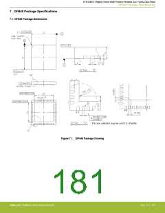
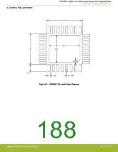
QFN48 Package Specifications
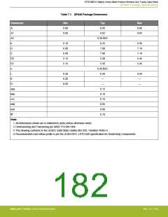
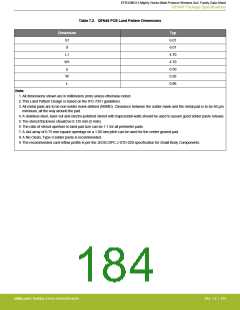
Table 7.2. QFN48 PCB Land Pattern Dimensions
Dimension
Typ
6.01
6.01
4.70
4.70
0.50
0.26
0.86
S1
S
L1
W1
e
W
L
Note:
1. All dimensions shown are in millimeters (mm) unless otherwise noted.
2. This Land Pattern Design is based on the IPC-7351 guidelines.
3. All metal pads are to be non-solder mask defined (NSMD). Clearance between the solder mask and the metal pad is to be 60 µm
minimum, all the way around the pad.
4. A stainless steel, laser-cut and electro-polished stencil with trapezoidal walls should be used to assure good solder paste release.
5. The stencil thickness should be 0.125 mm (5 mils).
6. The ratio of stencil aperture to land pad size can be 1:1 for all perimeter pads.
7. A 4x4 array of 0.75 mm square openings on a 1.00 mm pitch can be used for the center ground pad.
8. A No-Clean, Type-3 solder paste is recommended.
9. The recommended card reflow profile is per the JEDEC/IPC J-STD-020 specification for Small Body Components.
silabs.com | Building a more connected world.
Rev. 1.4 | 184

 SILICON [ SILICON ]