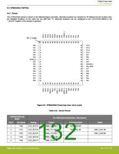
EFM32G Data Sheet
Pin Definitions
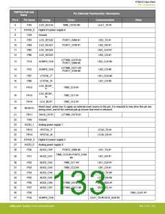
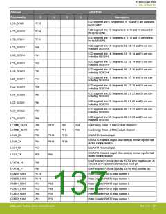
TQFP64 Pin# and
Name
Pin Alternate Functionality / Description
Pin #
6
Pin Name
PA5
Analog
Timers
TIM0_CDTI2 #0
Communication
Other
LCD_SEG18
LEU1_TX #1
7
IOVDD_0
VSS
Digital IO power supply 0.
Ground.
8
9
PB3
LCD_SEG20
LCD_SEG21
LCD_SEG22
LCD_SEG23
PCNT1_S0IN #1
US2_TX #1
US2_RX #1
US2_CLK #1
US2_CS #1
10
11
12
PB4
PCNT1_S1IN #1
PB5
PB6
LETIM0_OUT0 #3
PCNT1_S0IN #0
13
14
PC4
PC5
ACMP0_CH4
ACMP0_CH5
US2_CLK #0
US2_CS #0
LETIM0_OUT1 #3
PCNT1_S1IN #0
15
16
PB7
PB8
LFXTAL_P
LFXTAL_N
US1_CLK #0
US1_CS #0
LCD_BCAP_
P
17
PA12
TIM2_CC0 #1
LCD_BCAP_
N
18
19
20
PA13
PA14
TIM2_CC1 #1
TIM2_CC2 #1
LCD_BEXT
Reset input, active low.To apply an external reset source to this pin, it is required to only drive this pin low
during reset, and let the internal pull-up ensure that reset is released.
RESETn
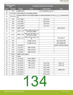
21
22
23
24
25
26
27
28
PB11
VSS
DAC0_OUT0
Ground.
LETIM0_OUT0 #1
AVDD_1
PB13
Analog power supply 1.
HFXTAL_P
LEU0_TX #1
LEU0_RX #1
PB14
HFXTAL_N
IOVDD_3
AVDD_0
PD0
Digital IO power supply 3.
Analog power supply 0.
ADC0_CH0
ADC0_CH1
PCNT2_S0IN #0
US1_TX #1
US1_RX #1
TIM0_CC0 #3 PCNT2_S1IN
#0
29
PD1
30
31
32
33
34
35
36
37
PD2
PD3
PD4
PD5
PD6
PD7
PD8
PC6
ADC0_CH2
ADC0_CH3
ADC0_CH4
ADC0_CH5
ADC0_CH6
ADC0_CH7
TIM0_CC1 #3
TIM0_CC2 #3
US1_CLK #1
US1_CS #1
LEU0_TX #0
LEU0_RX #0
I2C0_SDA #1
I2C0_SCL #1
LETIM0_OUT0 #0
LETIM0_OUT1 #0
CMU_CLK1 #1
ACMP0_CH6
LEU1_TX #0 I2C0_SDA #2
silabs.com | Building a more connected world.
Rev. 2.10 | 133

 SILICON [ SILICON ]