EFM32G Data Sheet
Pin Definitions
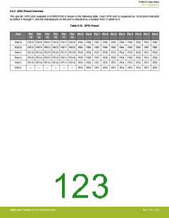
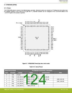
5.7 EFM32G840 (QFN64)
5.7.1 Pinout
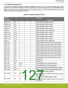
The EFM32G840 pinout is shown in the following figure and table. Alternate locations are denoted by "#" followed by the location num-
ber (Multiple locations on the same pin are split with "/"). Alternate locations can be configured in the LOCATION bitfield in the
*_ROUTE register in the module in question.
Figure 5.7. EFM32G840 Pinout (top view, not to scale)
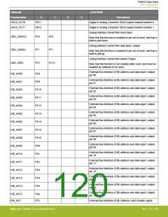
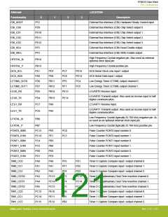
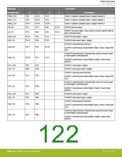
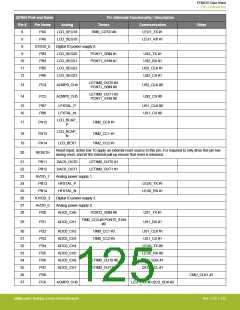
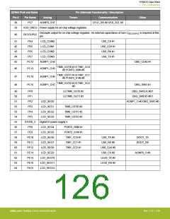
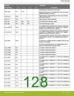
Table 5.19. Device Pinout
QFN64 Pin# and Name
Pin Alternate Functionality / Description
Pin #
Pin Name
VSS
Analog
Ground.
Timers
Communication
Other
0
1
2
3
4
5
PA0
LCD_SEG13
LCD_SEG14
LCD_SEG15
LCD_SEG16
LCD_SEG17
TIM0_CC0 #0/1
TIM0_CC1 #0/1
TIM0_CC2 #0/1
TIM0_CDTI0 #0
TIM0_CDTI1 #0
I2C0_SDA #0
I2C0_SCL #0
PA1
CMU_CLK1 #0
CMU_CLK0 #0
PA2
PA3
PA4
silabs.com | Building a more connected world.
Rev. 2.10 | 124

 SILICON [ SILICON ]