S102S01/S102S02/S202S01/S202S02
(
)
Ta = 25˚C
■ Electro-optical Characteristics
Parameter
Symbol
VF
Conditions
IF = 20mA
MIN.
TYP.
MAX.
1.4
Unit
V
Forward voltage
Input
-
-
1.2
4
Reverse current
IR
VR = 3V
-
-
-
-
-
10-
A
4
Repetitive peak OFF-state current
ON-state voltage
IDRM
VT
VD = VDRM
Resistance load
IF= 20mA, I T = 2Arms
-
10-
A
-
1.5
50
-
V rms
mA
V/µ s
Holding current
IH
-
-
Output
Critical rate of rise of OFF-state voltage
dV/dt
VD = 2/3 • V
30
DRM
Critical rate of rise of commutating
OFF-state voltage
T j = 125˚C, dI T /dt= - 4.0A/ms,
VD = 400V
(
)
C
dV/dt
V OX
5
-
-
V/µ s
S102S02
S202S02
Zero-cross voltage
Minimum
trigger
current
Isolation resistance
IF = 8mA
-
-
-
35
8
V
mA
mA
Ω
S102S01
S202S01
S102S02
S202S02
VD = 12V, R L = 30Ω
VD = 6V, R L = 30Ω
DC500V, 40 to 60 % RH
-
IFT
RISO
ton
-
-
8
Transfer
charac-
teristics
1010
-
-
S102S01
S202S01
S102S02
S202S02
-
-
-
-
-
-
1
ms
Turn-on
time
AC 50Hz
-
10
10
-
ms
Turn-off time
toff
-
-
-
-
ms
(
(
)
Thermal resistance
Thermal resistance
Between junction and case
Between junction and ambience
Rth
(
)
4.5
40
˚C/W
˚C/W
j - c
)
Rth
(
)
-
j - a
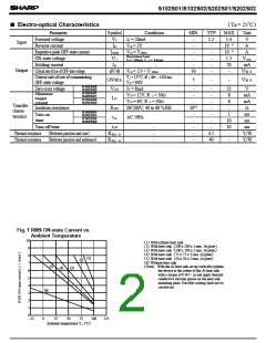
Fig. 1 RMS ON-state Current vs.
Ambient Temperature
10
(
(
(
(
(
(
(
)
)
)
)
)
)
1
2
3
4
5
6
With infinite heat sink
(
)
)
With heat sink 200 x 200 x 2 mm Al plate
9
8
(
With heat sink 100 x 100 x 2 mm Al plate
(
)
)
With heat sink 75 x 75 x 2 mm Al plate
( )
1
(
With heat sink 50 x 50 x 2 mm Al plate
( )
2
Without heat sink
)
7
6
5
4
3
2
1
( )
5
Note With the Al heat sink set up vertically,tighten
the device at the center of the Al heat sink
with a torque of 0.4N • m and apply thermal
conductive silicone grease on the heat sink
mounting plate. Forcible cooling shall not be
carried out.
( )
4
( )
3
( )
6
0
- 25
0
25
50
75
100
125
(
)
Ambient temperature T a ˚C

 SHARP [ SHARP ELECTRIONIC COMPONENTS ]