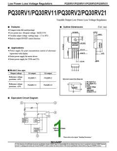
Low Power-Loss Voltage Regulators
PQ30RV1/PQ30RV11/PQ30RV2/PQ30RV21
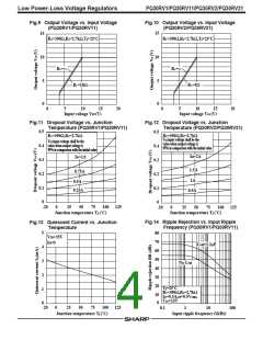
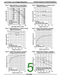
Fig.21 Output Peak Current vs. Junction
Temperature (PQ30RV2/PQ30RV21)
5
4
V
IN-V =5V
O
2V
3
2
0.5V
I
OP:Output current when output voltage
is 95% in comparison with the initial value
R1
=390Ω,R
25
Junction temperature T
2
=2.7kΩ
-20
0
50
75
100 125
(˚C)
j
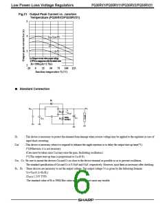
■ Standard Connection
D1
VO
VIN
1●
2●
4●
+
R
2
C
ref
+
3●
390Ω
to10kΩ
C
O
CIN
R1
D1
: This device is necessary to protect the element from damage when reverse voltage may be applied to the regulator in case of
input short-circuiting.
Cref
: This device is necessary when it is required to enhance the ripple rejection or to delay the output start-up time(*1).
(*1)Otherwise, it is not necessary.
(Care must be taken since Cref may raise the gain, facilitating oscillation.)
(*1)The output start-up time is proportional to Cre fX R2.
CIN, CO : Be sure to mount the devices CIN and CO as close to the device terminal as possible so as to prevent oscillation.
The standard specification of CIN and CO is 0.33µF and 47µF, respectively. However, ajust them as necessary after checking.
R1, R2 : These devices are necessary to set the output voltage. The output voltage VO is given by the following formula:
VO=Vref X (1+R2/R1)
(Vref is 1.25V TYP)
The standard value of R1 is 390Ω.But value up 10kΩdoes not cause any trouble.

 SHARP [ SHARP ELECTRIONIC COMPONENTS ]