Low Power-Loss Voltage Regulators
PQ05RF1 Series
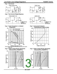
Fig.7 Output Voltage Minute Adjustment
Characteristics (PQ12RF1V)
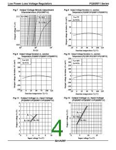
Fig.8 Output Voltage Deviation vs. Junction
Temperature (PQ05RF1/PQ05RF11/PQ05RF1V)
150
13.2
R1=390Ω
V
IN=7V
R1
=1kΩ
IO=0.5A
100
R1
=3.9kΩ
50
0
12.0
10.8
-50
-100
103
104
(Ω)
105
-25
0
25
50
75
100 125
(˚C)
R
2
Junction temperature T
j
Fig.10 Output Voltage Deviation vs. Junction
Temperature (PQ12RF1/PQ12RF11/PQ12RF1V)
250
Fig.9 Output Voltage Deviation vs. Junction
Temperature (PQ09RF1/PQ09RF11/PQ09RF1V)
200
150
100
50
V
IN=15V
VIN=18V
200
150
100
50
IO
=0.5A
I
O
=0.5A
0
-50
0
-50
-100
-150
-100
-150
-200
-25
0
25
50
75
100 125
j (˚C)
-25
0
25
50
75
100 125
j (˚C)
Junction temperature T
Junction temperature T
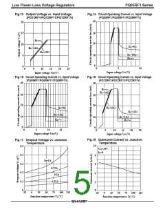
Fig.12 Output Voltage vs. Input Voltage
Fig.11 Output Voltage vs. Input Voltage
(PQ09RF1/PQ09RF11/PQ09RF1V)
(PQ05RF1/PQ05RF11/PQ05RF1V)
10
8
7
6
RL=∞
5
4
3
2
R =∞
L
RL
=18Ω
5
0
RL
=5Ω
RL=9Ω
RL
=10Ω
1
0
0
2
4
6
8
10
0
5
10
15
Input voltage VIN (V)
Input voltage VIN (V)

 SHARP [ SHARP ELECTRIONIC COMPONENTS ]