PC929
(Ta=Topr unless otherwise specified)
MIN. TYP. MAX. Unit Test circuit
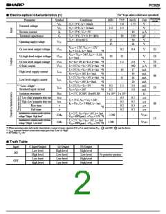
■ Electro-optical Characteristics (2)
Parameter
Symbol
Conditions
*9
*10 Overcurrent detecting voltage
VCTH
VCC
-
VCC
-
VCC -
Ta = 25˚C, IF = 5mA
V
V
( )
9
VCC = V01 = 24V, RG = 47Ω
CG = 3 000pF, FS= OPEN
6.5
1
6.0
2
5.5
3
Overcurrent detecting voltage
hysteresis width
VCHIS
*9
O2 "High→Low" delay time
tPCOHL
tPCOtf
VOE
-
2
-
4
5
-
10
-
Ta = 25˚C
µ s
µ s
at protection from overcurrent
(
)
13
VCC = V01 = 24V, IF = 5mA
CG = 3 000pF, RG = 47Ω
CP = 1 000pF, RC = 1kΩ
FS= OPEN
O2 fall time at protection
from overcurrent
O2 output voltage at protection
from overcurrent
( )
10
2
V
V
*9
T
a = 25˚C, IF = 5mA, IFS = 10mA
Low level error
signal voltage
( )
11
VFSL
VCC = VO1 = 24V, RG = 47Ω , CG = 3 000pF,
-
0.2
0.4
C = OPEN
T
V
a = 25˚C, IF = 5mA, VFS = 24V
CC = VO1 = 24V, RG = 47Ω , CG = 3 000pF,
High level error
signal current
( )
12
IFSH
-
-
-
100
µ A
VC = 0V
Error signal "High→Low"
delay time
Ta = 25˚C, RFS = 1.8kΩ
VCC = VO1 = 24V, IF = 5mA
CG = 3 000pF, RG = 47Ω
CP = 1 000pF, RC = 1kΩ
tPCFHL
1
5
-
µ s
µ s
(
)
14
Error signal output pulse width
∆ tFS
20
35
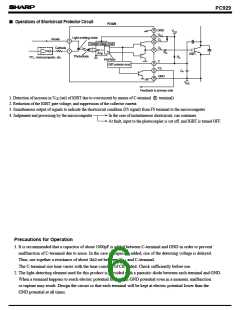
*9 When measuring overcurrent, protective output and error signal output characteristics, connect a bypass capacitor (0.01 µ F or more) between V
CC
13 and GND 14 near the device.
*10 V
represents C-terminal voltage when O output goes from "High" to "Low".
CTH
2
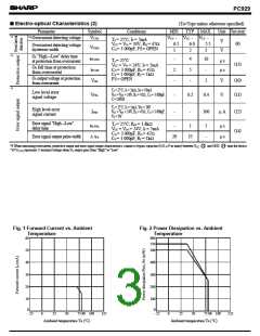
Fig. 1 Forward Current vs. Ambient
Fig. 2 Power Dissipation vs. Ambient
Temperature
Temperature
60
600
550
500
50
40
30
20
400
300
200
10
0
100
0
- 25
0
25
50
75 80 100
125
- 25
0
25
50
75 80 100
125
Ambient temperature Ta (˚C)
Ambient temperature Ta (˚C)

 SHARP [ SHARP ELECTRIONIC COMPONENTS ]