PC457L0NIP
(Ta=25˚C)
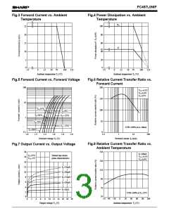
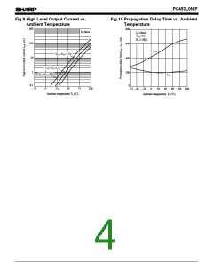
ꢀ Electro-optical Characteristics
Parameter
Symbol
VF
Conditions
IF=16mA
MIN.
−
TYP. MAX.
Unit
V
Forward voltage
1.7
−
1.95
10
Input
Reverse current
IR
VR=5V
−
µA
pF
Terminal capacitance
Ct
VF=0V, f=1MHz
−
60
3
250
500
1.0
50
High level output current (1)
High level output current (2)
*6 High level output current (3)
High level supply current (1)
*6 High level supply current (2)
Low level supply current
Low level output voltage
IOH (1)
IOH (2)
IOH (3)
ICCH (1)
ICCH (2)
ICCL
IF=0, VCC=5.5V, VO=5.5V
IF=0, VCC=15V, VO=15V
IF=0, VCC=15V, VO=15V
IF=0, VCC=15V, VO=open
IF=0, VCC=15V, VO=open
IF=16mA, VCC=15V, VO=open
IF=16mA, VCC=4.5V, IO=2.4mA
IF=16mA, VCC=4.5V, VO=0.4V
IF=16mA, VCC=4.5V, VO=0.4V
−
nA
µA
µA
µA
µA
µA
−
−
−
−
Output
−
1.0
2.0
−
0.02
−
−
−
120
−
VOL
CTR (1)
CTR (2)
tPHL
−
0.4
50
V
%
Current transfer ratio (1)
*6 Current transfer ratio (2)
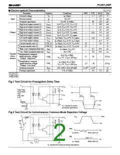
*7 "High→Low" propagation delay time
*7 "Low→High" propagation delay time
19
15
−
−
−
−
%
µs
µs
0.2
0.6
0.8
0.8
IF=16mA, VCC=5V
RL=1.9Ω
tPLH
−
*8 Instantaneous common
mode rejection voltage
"Output : High level"
*8 Instantaneous common
mode rejection voltage
"Output : Low level"
Transfer
charac-
teristics
IF=0, RL=1.9kΩ
VCC=5V, VCM=1.0kV(p-p)
15
30
−
−
kV/µs
kV/µs
CMH
CML
IF=16mA, RL=1.9kΩ
VCC=5V, VCM =1.0kV(p-p)
−15
−30
Isolation resistance
Floating capacitance
RISO
Cf
DC=500V, 40 to 60%RH
V=0, f=1MHz
5×10¹⁰ 1×10¹¹
0.6
−
Ω
−
1.0
pF
*6 Ta=0 to 70°C
*7 Refer to Fig.1
*8 Refer to Fig.2
Fig.1 Test Circuit for Propagation Delay Time
IF
IF
VCC
Pulse input
Pulse width
10µs
Duty ratio
1/10
RL
0V
VO
tPHL
tPLH
CL
IF
VO
5V
Monitor
1.5V
VOL
*CL includes the probe
and wiring capacitance.
100Ω
Fig.2 Test Circuit for Instantaneous Common Mode Rejection Voltage
IF
VCM
1.0kV
VCC
SW
B
RL
A
0V
VO
CMH
CML
VO
5V
2V
(IF=0mA)
When SW is A
CL
GND
0.8V
When SW is B
VO
+
−
VOL
(IF=16mA)
VCM
*CL includes the probe and wiring capacitance.

 SHARP [ SHARP ELECTRIONIC COMPONENTS ]