PC410
(
)
Ta= 0 to + 70˚C unless otherwise specified
■ Electro-optical Characteristics
Parameter
Symbol
VF
Conditions
Ta= 25˚C, I F = 10mA
Ta= 25˚C, V R = 5V
MIN.
TYP.
1.6
-
MAX.
1.9
10
150
0.6
250
18
15
Unit
V
Forward voltage
-
-
-
-
-
-
-
-
Input
Reverse current
IR
µ A
pF
Terminal capacitance
Ct
Ta= 25˚C, V= 0, f= 1MH
60
0.4
2
Z
Low level output voltage
High level output current
Low level supply current
High level supply current
“ H→L” threshold input current
Isolation resistance
V OL
IOH
IOL = 13mA, VCC = 5.5V, I F = 5mA
VCC = VO = 5.5V, I F = 250m A
VCC = 5.5V, I F = 10mA
VCC = 5.5V, I F = 0
V
µ A
mA
mA
mA
Ω
Output
ICCL
ICCH
I FHL
RISO
Cf
13
7
2.5
1011
0.6
5
VCC = 5V, V O = 0.8V, RL = 350Ω
Ta = 25˚C, DC500V, 40 to 60% RH
Ta= 25˚C, V= 0, f= 1MHz
5 x 10¹⁰
-
-
-
pF
Floating capacitance
“ H→L” propagation
delay time
-
-
50
50
120
120
t PHL
t PLH
Ta= 25˚C
V
CC = 5V, I F = 7.5mA
“ L→H” propagation
delay time
ns
RL = 350Ω , C L = 15pF
-
-
30
30
60
60
Fall time
tf
tr
Transfer
charac-
teristics
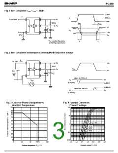
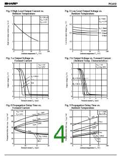
Fig. 1
Rise time
Instantaneous common
mode rejection
voltage “ High level
output”
IF = 0
Ta= 25˚C
(
)
100
500
-
-
CMH
VO MIN. = 2V
V
CC = 5V
V/ µ s
(
)
VCM = 10V Peak
RL = 350Ω
Fig. 2
Instantaneous common
mode rejection
voltage “ Low level
output”
IF = 5mA
(
)
- 100
- 500
CML VO MAX. = 0.8V
)
Note All typical values : at Ta= 25˚C, VCC = 5V
Each characteristics shall be measured under opaque condition.
■ Recommended Operation Conditions
Parameter
Low level input current
Symbol MIN.
MAX.
250
15
Unit
µ A
mA
V
IFL
IFH
VCC
N
0
7
High level input current
Supply voltage
4.5
-
5.5
8
(
)
Fanout
TTL load
-
Operating temperature
T opr
0
70
˚C
(
)
Connect a by-pass ceramic capacitor 0.01 to 0.1µ F between VCC and GND at the
position within 1cm from lead pin.

 SHARP [ SHARP ELECTRIONIC COMPONENTS ]