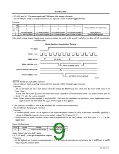
STK672-080
Continued from preceding page.
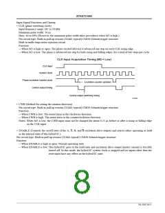
• The CLK input pin include built-in malfunction
prevention circuits for external pulse noise.
• Both an ENABLE and RESET pin are provided as
Schmitt trigger inputs with built-in 20 kΩ (typical) pull-
up resistors.
to provide microstepping operation even for small motor
currents.
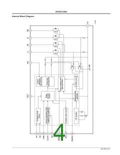
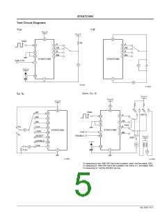
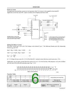
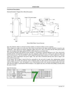
<Driver Block>
• Provides a wide range of operatng supply voltage
required for external excitation PWM drive (V 1 = 10
CC
• No audible noise is generated by the differences in the
time constant between phases A and B when the motor
position is held fixed due to the adoption of external
excitation.
to 45 V).
• Current detection resistor (0.15 Ω) built-in the hybrid IC
itself.
• Power MOSFETs adopted for low drive loss
• The reference voltage Vref can be set to any level
• Provides a motor output drive current of I
(When Tc = 105°C).
= 2.8 A
OH
between 0 and 1/2 V 2. This allows the STK672-080
CC
Specifications
Absolute Maximum Ratings at Tc = 25°C
Parameter
Maximum supply voltage1
Maximum supply voltage2
Input voltage
Symbol
Conditions
Ratings
52
Unit
V
V
CC1 max No signal
CC2 max No signal
V
–0.3 to +7.0
V
V
IN max
Logic input pins
–0.3 to +7.0
V
Phase output current
Repeatable avalanche current
Power loss
I
OH max
0.5 s, 1 pulse, when VCC1 applied.
3.3
A
Ear max
Pd max
Tc max
Tj max
Tstg
30
mJ
W
°C
°C
°C
θc-a = 0
8
105
Operating substrate temperature
Junction temperature
Storage temperature
150
–40 to +125
Allowable Operating Ranges at Ta = 25°C
Parameter
Symbol
Conditions
With input signals present
Ratings
10 to 45
5 ±5%
Unit
V
Supply voltage1
Supply voltage2
Input voltage
V
V
CC1
CC2
With input signals present
V
VIH
0 to VCC
2
V
Phase driver voltage handling
Phase current 1
VDSS
Tr1, 2, 3, and 4 (the A, A, B, and B outputs)
Tc = 105°C, CLK ≥ 200 Hz
100 (min)
V
I
I
OH 1
OH 2
2.8
3
A
Phase current 2
Tc = 80°C, CLK ≥ 200 Hz
A
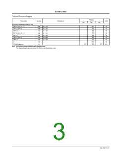
Electrical Characteristics at Tc = 25°C, V 1 = 24 V, V 2 = 5 V
CC
CC
Ratings
typ
2.1
Parameter
Symbol
Conditions
Unit
min
0.445
4
max
Control supply current
Output saturation voltage
Average output current
FET diode Forward voltage
[Control Inputs]
ICC
Vsat
Io ave
Vdf
Pin 6 input, with ENABLE pin held low.
RL = 12 Ω
14
1
mA
V
0.65
0.5
1
Load: R = 3.5 W/L = 3.8 mH per phase
If = 1 A
0.56
1.5
A
V
VIH
VIL
IIH
Except for the Vref pin
Except for the Vref pin
Except for the Vref pin
Except for the Vref pin
V
V
Input voltage
Input current
1
10
0
1
µA
µA
IIL
125
250
510
[Vref Input Pin]
Input voltage
VI
II
Pin 7
0
2.5
V
Input current
Pin 7, 2.5-V input
330
415
545
µA
[Control Outputs]
VOH
VOL
I = –3 mA, pin MOI
I = +3 mA, pin MOI
2.4
V
V
Output voltage
0.4
Continued on next page.
No. 6507-2/17

 SANYO [ SANYO SEMICON DEVICE ]