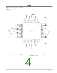
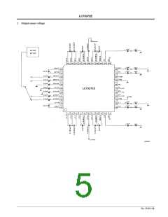
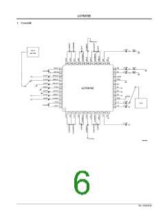
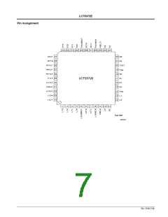
LC75372E
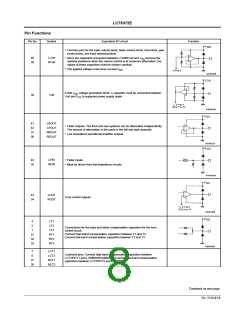
Pin Functions
Pin No.
Symbol
Equivalent I/O circuit
Function
• Common pins for the main volume block, fader volume block, tone block, gain
control block, and input switching block.
40
38
LVref
RVref
• Since the capacitors connected between LVref/RVref and V become the
SS
residual resistance when the volume control is at maximum attenuation, the
values of these capacitors must be chosen carefully.
• The applied voltage must never exceed V
.
DD
0.488 V
voltage generation block. A capacitor must be connected between
DD
39
Vref
Vref and V to suppress power supply ripple.
SS
41
42
37
36
LROUT
LFOUT
RROUT
RFOUT
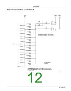
• Fader outputs. The front and rear systems can be attenuated independently.
The amount of attenuation is the same in the left and right channels.
• Low impedance operational amplifier outputs
43
35
LFIN
RFIN
• Fader inputs
• Must be driven from low-impedance circuits.
44
34
LOUT
ROUT
Tone control outputs
3
2
LT1
LT2
LT3
RT1
RT2
RT3
Connections for the bass and treble compensation capacitors for the tone
control circuit
Connect high-band compensation capacitors between T1 and T2.
Connect low-band compensation capacitors between T2 and T3.
1
31
32
33
7
6
LCT1
LCT2
RCT1
RCT2
Loudness pins. Connect high-band compensation capacitors between
LCT1/RCT1 and L10dBIN/R10dBIN, and connect low-band compensation
capacitors between LCT2/RCT2 and LVref/RVref.
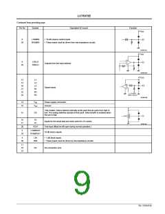
27
28
Continued on next page.
No. 5330-8/18

 SANYO [ SANYO SEMICON DEVICE ]