LA4261
Note for Changing Voltage Gain
Basically, the voltage gain can be reduced by adding external
resistors (RNF) in series with feedback capacitors C1, C4.
However, it should be noted that since there is no phase
compensation pin the frequency response is extended and
oscillation is liable to occur when the voltage gain is reduced.
The voltage gain must not be reduced to be less than 30 dB.
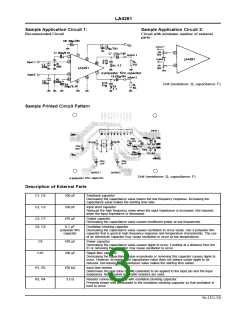
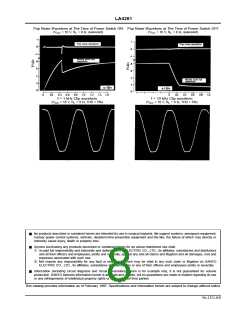
External Muting
If external muting is required, make the circuit as shown right.
In this case, the attack time, recovery time, and pop noise are
similar to those which occur at the time of power switch
ON/OFF.
Unit (resistance: Ω, capacitance: F)
Proper Cares in Using IC
.
Maximum ratings
If the IC is used in the vicinity of the maximum ratings, even a slight variation in conditions may cause the maximum ratings to
be exceeded, thereby leading to breakdown. Allow an ample margin of variation for supply voltage, etc. and use the IC in the
range where the maximum ratings are not exceeded.
.
Pin-to-pin short
If power is applied when the space between pins is shorted, breakdown or deterioration may occur. When mounting the IC on
the board or applying power, make sure that the space between pins is not shorted with solder, etc.
.
.
When using in radios, allow a sufficient space between IC and bar antenna.
Printed circuit pattern
When designing the printed circuit pattern, make the power supply, output, and ground lines thick and short and arrange the
pattern and parts so that no feedback loop is formed between input and output. Place power capacitor C9, oscillation blocking
capacitors C6, C8 as close to IC pins as possible to prevent oscillation from occurring. Refer to the sample printed circuit
pattern.
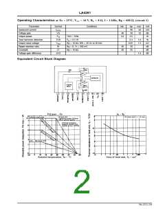
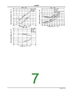
PO – VIN
THD – PO
Input voltage, VIN – mV
Output power, PO – W
No.1321-4/8

 SANYO [ SANYO SEMICON DEVICE ]