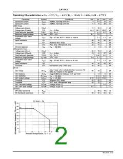
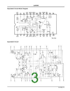
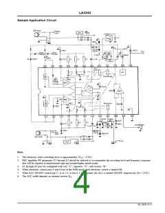
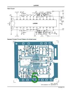
LA3242
IC usage Notes
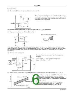
(1) The base of a PNP transistor is connected to input pins 2 and 23.
When a voltage is applied to input pins 2 and 23 externally, connect a
capacitor to the input pins. The recommended value of capacitor C is
0.1 µF to 10 µF. DC voltage VINDC with input pins 2 and 23 open is
50 mV max (VINDC = 20 mV typ).
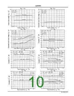
For the relation between supply voltage VCC and VINDC, refer to the VCC – VINDC characteristic.
(2) Output waveform starting time (Refer to Data ts – Cr.)
Rise waveform at pin 7 or 18
When supply voltage VCC is switched ON, the amplifier output (pins 7 and 18) will rise. Output waveform ON time ts can be
varied by capacitor Cr connected to pin 12. The minimum value of Cr is 33 µF. If the value of Cr is made less than 33 µF, more
pop noise will occur and the ripple rejection will worsen at the time supply voltage VCC is switched ON. (ts = 0.7 s. typ at
Cr = 100 µF)
(3) Electronic switch control circuit
The control circuit for control pins 9 and 16 is configured as
shown left.
Electronic
Control level VCONT of the control circuit is given by:
VCONT = 1/2 × (VCC – 0.9) [V]
SW ON
signal
Control
pin
. 4 µAmin
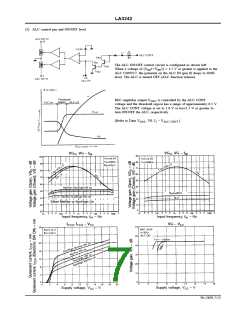
(4) Relation between control voltage to turn ON/OFF electronic switch and supply voltage (Refer to Data VCONT – VCC.)
The control level at electronic switch CONT pin 9 and 16 is fixed
by supply voltage VCC. The threshold region has a range of
approximately 1 V. The middle point of threshold region at a
given value of supply voltage VCC is represented by approximately
Electronic SW OFF
1/2 × (VCC – 0.9) V.
Electronic SW ON
The electronic switch can be turned ON/OFF by applying a
voltage of the middle point voltage ±0.5 V or more/less,
respectively, to electronic switch CONT pins 9 and 16.
Threshold region (. 1 V)
No.2620-6/12

 SANYO [ SANYO SEMICON DEVICE ]