60V N -ch MOSFET
2SK3711
December 2005
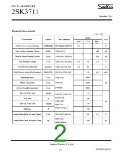
Electrical characteristics
(Ta=25°C)
Limits
TYP
Characteristic
Symbol
Test Conditions
Unit
MIN
60
MAX
Drain to Source breakdown Voltage
Gate to Source Leakage Current
Drain to Source Leakage Current
Gate Threshold Voltage
Forward Transconductance
Static Drain to Source On-Resistance
Input Capacitance
V(BR)DSS ID=100μA,VGS=0V
V
μA
μA
V
IGSS
IDSS
VGS=±15V
±10
100
4.0
VDS=60V, VGS=0V
VDS=10V, ID=1mA
VDS=10V, ID=35A
VTH
2.0
30
3.0
80
Re(Yfs)
S
RDS(ON) ID=35A, VGS=10V
5.0
6.0
mΩ
Ciss
Coss
Crss
td(on)
tr
8000
1250
1000
110
100
440
160
0.9
VDS=10V
VGS=0V
f=1MHz
Output Capacitance
pF
Reverse Transfer Capacitance
Turn-On Delay Time
ID=35A, VDD≈20V
RL=0.57Ω,
Rise Time
VGS=10V
ns
Turn-Off Delay Time
td(off)
tf
Rg=22Ω
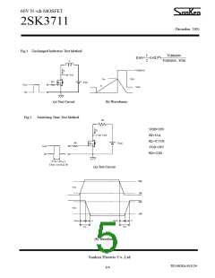
Refer to Fig. 2
Fall Time
Source-Drain Diode Forward Voltage
VSD
ISD=50A,VGS=0V
1.5
V
ISD=25A,
Source-Drain Diode Recovery Time
trr
100
ns
di/dt=50A/μs
Sanken Electric Co.,Ltd.
T02-002EA-051124
2/9

 SANKEN [ SANKEN ELECTRIC ]