S3C4510B
SYSTEM MANAGER
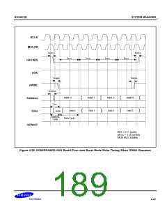
ROM BANK 5 ADDRESS/DATA MULTIPLEXED BUS
Overview
The S3C4510B has separate address and data bus. S3C4510B supports multiplexed address/data bus for low
cost chips which require multiplexed bus. To support this feature, the S3C4510B has one special bank (ROM
bank 5) which can support address/data multiplexed bus and 4-data burst access by GDMA. For this feature, you
should set the MUX enable bit and wait enable bit of CLKCON register.
You can also use ROM bank 5 as normal ROM bank by clearing MUX enable bit of CLKCON register.
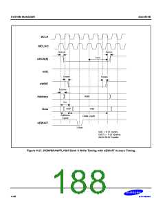
When you set the wait enable bit in the CLKCON register, wait cycle can be added by nEWAIT pin for ROM bank
5. Other ROM banks except ROM bank 5 has no effects. nEWAIT pin also can be used to add wait cycle for EXT
I/O bank regardless of the wait enable bit.
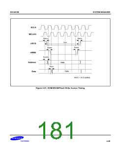
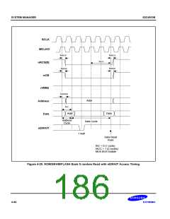
Random Access by CPU
At the first cycle of ROM bank 5, address comes out from data bus. Therefore, any device which is connected to
the ROM bank 5 can get address. The rest cycle is for data. As the S3C4510B has not a dedicated address
strobe signal for address phase in the data burst, you should generate address strobe signal in the application
device.
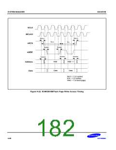
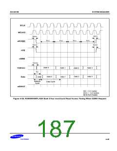
Four-data Burst Access by GDMA
When you set FB (4-data burst enable) bit in the GDMACON register, the GDMA requests 4-data burst access.
When you access ROM bank 5 by 4-data burst mode, the multiplexed ROM bank 5 bus has only one address
phase. Therefore, you should internally calculate the address at the data phase. To notify the 4-data burst mode
to ROM bank 5 device, the ADDR[21] remains "1" during address phase.
4-43

 SAMSUNG [ SAMSUNG ]