MultiMediaCardTM
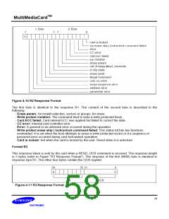
Error
Illegal
Command
Card ECC
Failed
‘1’ = error
‘0’ = no error
‘1’ = error
‘0’ = success
‘1’ = failure
‘0’ = no error
‘1’ = error
‘0’ = no error
‘1’ = error
‘0’ = not
protected
‘1’ = protected
‘0’ = no error
‘1’ = error
command failed.
Command not legal for the card
state.
Card internal ECC was applied
but failed to correct the data.
Internal card controller error.
E R
C
C
C
C
C
R1 R2
E X
R2
DataErr
R2
DataErr
R2
E R X
E R X
S X
CC Error
Error
A general or an unknown error
occurred during the operation.
Only partial address space was
erased due to existing WP
blocks.
Sequence or password error
during card lock/unlock
operation.
DaraErr
R2
WP Erase Skip
E X
S X
C
A
Lock/Unlock
Command
R2
Card is locked
Erase Retest
In Idle State
R2
DaraErr
‘0’ = card is
not locked
‘1’ = card is
locked
‘0’ = cleared
‘1’ = set
Card is locked by password.
S R
S R
C
A
R1 R2
R1 R2
An erase sequence was cleared
before exciting because an
output of erase sequence
command was received.
The card enters the idle state
after power up or reset
‘0’ = Card is
ready
‘1’ = protected
command. It will exit this state
and become ready upon
completion of this initialization
procedures.
E X
C
CSD Overwrite
R2
‘0’ = no error
‘1’ = error
The host is trying to change the
ROM section, or is trying to
reserve the copy bit (set as
original) or permanent WP bit
(unprotected) or the CSD
register.
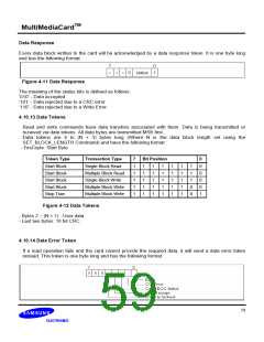
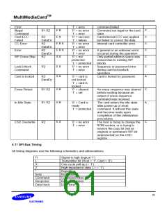
4.11 SPI Bus Timing
All timing diagrams use the following schematics and abbreviations:
H
L
X
Z
Signal is high (logical ‘1’)
Transmitter bit (Host = ‘1’, Card = ‘0’)
One-cycle pull-up (= ‘1’)
High impedance state (-> = ‘1’)
Repetition
*
busy
Busy token
Command
Response
Data block
Command token
Response token
Data token
61

 SAMSUNG [ SAMSUNG ]