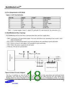
MultiMediaCardTM
4.5.3 Relative Card Address (RCA)
The 16-bit relative card address register carries the card address assigned by the host during the card
identification. This address is used for the addressed host to card communication after the card
identification procedure. The default value of the RCA register is 0x0001. The value 0x0000 is reserved
to set all cards in Standby State with the command SELECT_DESELECT_CARD (CMD7). The RCA is
programmed with the command SET_RELATIVE_ADDRESS (CMD3) during the initialization
procedure. The content of this register is lost after power down. The default value is assigned when an
internal reset is applied by the power up detection unit of the MultiMediaCard.
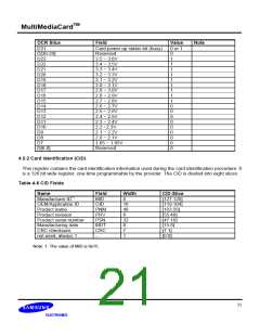
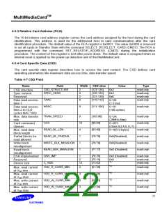
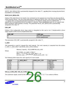
4.5.4 Card Specific Data (CSD)
The card specific data register describes how to access the card content. The CSD defines card
operating parameters like maximum data access time, data transfer speed.
Table 4-7 CSD Field
Name
Field
CSD_STRUCTURE
SPEC_VERS
--
Width
CSD-slice
[127:126]
[125:122]
[121:120]
[119:112]
Value
Type
read only
read only
read only
read only
2
0x2
0x3
0x0
CSD structure
Spec version
Reserved
Data read access-
time-1
4
2
8
TAAC
0×26
(1.5 ms)
NSAC
8
[111:104]
read only
0×01
(100 cycles)
Data read access-
time-2 in CLK
cycles NAC*100)
Max. data transfer
rate
TRAN_SPEED
8
[103:96]
[95:84]
[83:80]
[79:79]
[78:78]
[77:77]
read only
read only
read only
read only
read only
read only
0×2A
(20MHz,Max)
0×0F5
(Class 0,2,4,5, 6, 7)
0×9(512 bytes)
CCC
12
4
Card command
classes
READ_BL_LEN
Max. read data
block length
Partial blocks for
read allowed
Write block
misalignment
Read block
misalignment
DSR implemented
Reserved
READ_BL_PARTIAL
WRITE_BLK_MISALIGN
READ_BLK_MISALIGN
1
0x0(Disabled)
0x0(Disabled)
0x0 (Disabled)
0x0 (Disabled)
1
1
DSR_IMP
--
C_SIZE
1
2
12
[76:76]
[75:74]
[73:62]
read only
read only
read only
0x0
*1
Device size
*2
*2
*2
*2
VDD_R_CURR_MIN
VDD_R_CURR_MAX
VDD_W_CURR_MIN
VDD_W_CURR_MAX
3
3
3
3
[61:59]
[58:56]
[55:53]
[52:50]
read only
read only
read only
read only
Max. read current
at VDD min
Max. read current
at VDD max
Max. write current
at VDD min
Max. write current
at VDD max
22

 SAMSUNG [ SAMSUNG ]