Preliminary
K5A3x80YT(B)C
MCP MEMORY
Read While Write
Flash memory provides dual bank memory architecture that divides the memory array into two banks. The device is capable of read-
ing data from one bank and writing data to the other bank simultaneously. This is so called the Read While Write operation with dual
bank architecture; this feature provides the capability of executing the read operation during Program/Erase or Erase-Suspend-Pro-
gram operation.
The Read While Write operation is prohibited during the chip erase operation. It is also allowed during erase operation when either
single block or multiple blocks from same bank are loaded to be erased. It means that the Read While Write operation is prohibited
when blocks from Bank1 and another blocks from Bank2 are loaded all together for the multi-block erase operation.
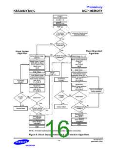
Block Group Protection & Unprotection
Flash memory feature hardware block group protection. This feature will disable both program and erase operations in any combina-
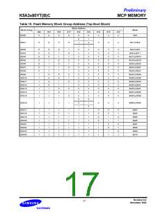
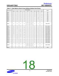
tion of twenty five block groups of memory. Please refer to Tables 10 and 11. The block group protection feature is enabled using
programming equipment at the user’s site. The device is shipped with all block groups unprotected.
This feature can be hardware protected or unprotected. If a block is protected, program or erase command in the protected block will
be ignored by the device. The protected block can only be read. This is useful method to preserve an important program data. The
block group unprotection allows the protected blocks to be erased or programed. All blocks must be protected before unprotect oper-
ation is executing. The block protection and unprotection can be implemented by the following method.
Table 9. Block Group Protection & Unprotection
DQ15/
A-1
DQ8/
DQ14
DQ0/
DQ7
CEF
BYTEF
Operation
OE
WE
A9
A6
A1
A0
RESET
Block Group Protect
L
L
H
H
L
L
X
X
X
X
L
H
H
L
L
X
X
X
X
DIN
DIN
VID
VID
Block Group Unprotect
H
Address must be inputted to the block group address (A12~A20) during block group protection operation. Please refer to Figure 9
(Algorithm) and Switching Waveforms of Block Group Protect & Unprotect Operations.
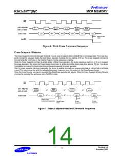
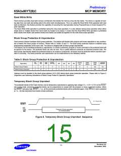
Temporary Block Group Unprotect
The protected blocks of the Flash memory can be temporarily unprotected by applying high voltage (VID = 8.5V~12.5V) to the RESET
ball. In this mode, previously protected blocks can be programmed or erased with the program or erase command routines. When
the RESET ball goes high (RESET = VIH), all the previously protected blocks will be protected again. If the WP/ACC ball is asserted
at VIL , the two outermost boot blocks remain protected.
VID
V = VIH or VIL
RESET
CE
F
Program & Erase operation
at Protected Block
WE
Figure 8. Temporary Block Group Unprotect Sequence
Revision 0.0
November 2002
- 15 -

 SAMSUNG [ SAMSUNG ]