Rev. 1.01
K4B2G0446D
K4B2G0846D
datasheet
DDR3L SDRAM
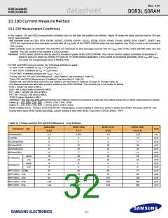
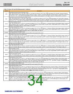
[ Table 33 ] Basic IDD and IDDQ Measurement Conditions
Symbol
Description
Operating One Bank Active-Precharge Current
CKE: High; External clock: On; tCK, nRC, nRAS, CL: see Table 32 on page 32 ; BL: 8 ; AL: 0; CS: High between ACT and PRE; Command, Address,
Bank Address Inputs: partially toggling according to Table 32 on page 31 ; Data IO: FLOATING; DM:stable at 0; Bank Activity: Cycling with one bank active
1)
IDD0
IDD1
2)
at a time: 0,0,1,1,2,2,... (see Table 32); Output Buffer and RTT: Enabled in Mode Registers ; ODT Signal: stable at 0; Pattern Details: see Table 32
Operating One Bank Active-Read-Precharge Current
CKE: High; External clock: On; tCK, nRC, nRAS, nRCD, CL: see Table 32 on page 32 ; BL: 8 ; AL: 0; CS: High between ACT, RD and PRE; Command,
Address, Bank Address Inputs, Data IO: partially toggling according to Table 33 on page 32 ; DM:stable at 0; Bank Activity: Cycling with one bank active at
1)
2)
a time: 0,0,1,1,2,2,... (see Table 33); Output Buffer and RTT: Enabled in Mode Registers ; ODT Signal: stable at 0; Pattern Details: see Table 33
Precharge Standby Current
1)
CKE: High; External clock: On; tCK, CL: see Table 32 on page 32 ; BL: 8 ; AL: 0; CS: stable at 1; Command, Address, Bank Address Inputs: partially tog-
IDD2N
gling according to Table 34 on page 32 ; Data IO: FLOATING; DM:stable at 0; Bank Activity: all banks closed; Output Buffer and RTT: Enabled in Mode
2)
Registers ; ODT Signal: stable at 0; Pattern Details: see Table 34
Precharge Standby ODT Current
1)
CKE: High; External clock: On; tCK, CL: see Table 32 on page 32 ; BL: 8 ; AL: 0; CS: stable at 1; Command, Address, Bank Address Inputs: partially tog-
IDD2NT
IDDQ2NT
IDD2P0
gling according to Table 35 on page 33 ; Data IO: FLOATING;DM:stable at 0; Bank Activity: all banks closed; Output Buffer and RTT: Enabled in Mode
2)
Registers ; ODT Signal: toggling according to Table 35 ; Pattern Details: see Table 35
Precharge Standby ODT IDDQ Current
Same definition like for IDD2NT, however measuring IDDQ current instead of IDD current
Precharge Power-Down Current Slow Exit
CKE: Low; External clock: On; tCK, CL: see Table 32 on page 32 ; BL: 8 ; AL: 0; CS: stable at 1; Command, Address, Bank Address Inputs: stable at 0;
1)
2)
Data IO: FLOATING; DM:stable at 0; Bank Activity: all banks closed; Output Buffer and RTT: Enabled in Mode Registers ; ODT Signal: stable at 0; Pre-
3)
charge Power Down Mode: Slow Exi
Precharge Power-Down Current Fast Exit
CKE: Low; External clock: On; tCK, CL: see Table 32 on page 32; BL: 8 ; AL: 0; CS: stable at 1; Command, Address, Bank Address Inputs: stable at 0;
1)
IDD2P1
IDD2Q
IDD3N
IDD3P
2)
Data IO: FLOATING; DM:stable at 0; Bank Activity: all banks closed; Output Buffer and RTT: Enabled in Mode Registers ; ODT Signal: stable at 0; Pre-
3)
charge Power Down Mode: Fast Exit
Precharge Quiet Standby Current
1)
CKE: High; External clock: On; tCK, CL: see Table 32 on page 32 ; BL: 8 ; AL: 0; CS: stable at 1; Command, Address, Bank Address Inputs: stable at 0;
Data IO: FLOATING; DM:stable at 0;Bank Activity: all banks closed; Output Buffer and RTT: Enabled in Mode Registers ; ODT Signal: stable at 0
2)
Active Standby Current
1)
CKE: High; External clock: On; tCK, CL: see Table 32 on page 32 ; BL: 8 ; AL: 0; CS: stable at 1; Command, Address, Bank Address Inputs: partially tog-
gling according to Table 34 on page 32 ; Data IO: FLOATING; DM:stable at 0;Bank Activity: all banks open; Output Buffer and RTT: Enabled in Mode
2)
Registers ; ODT Signal: stable at 0; Pattern Details: see Table 34
Active Power-Down Current
1)
CKE: Low; External clock: On; tCK, CL: see Table 32 on page 32 ; BL: 8 ; AL: 0; CS: stable at 1; Command, Address, Bank Address Inputs: stable at 0;
Data IO: FLOATING;DM:stable at 0; Bank Activity: all banks open; Output Buffer and RTT: Enabled in Mode Registers ; ODT Signal: stable at 0
2)
Operating Burst Read Current
1)
CKE: High; External clock: On; tCK, CL: see Table 32 on page 32 ; BL: 8 ; AL: 0; CS: High between RD; Command, Address, Bank Address Inputs: par-
IDD4R
IDDQ4R
IDD4W
tially toggling according to Table 36 on page 33 ; Data IO: seamless read data burst with different data between one burst and the next one according to
Table 36 ; DM:stable at 0; Bank Activity: all banks open, RD commands cycling through banks: 0,0,1,1,2,2,... (see Table 7 on page 12); Output Buffer and
2)
RTT: Enabled in Mode Registers ; ODT Signal: stable at 0; Pattern Details: see Table 36
Operating Burst Read IDDQ Current
Same definition like for IDD4R, however measuring IDDQ current instead of IDD current
Operating Burst Write Current
1)
CKE: High; External clock: On; tCK, CL: see Table 32 on page 32 ; BL: 8 ; AL: 0; CS: High between WR; Command, Address, Bank Address Inputs: par-
tially toggling according to Table 37 on page 34 ; Data IO: seamless write data burst with different data between one burst and the next one according to
Table 37; DM: stable at 0; Bank Activity: all banks open, WR commands cycling through banks: 0,0,1,1,2,2,... (see Table 37); Output Buffer and RTT:
2)
Enabled in Mode Registers ; ODT Signal: stable at HIGH; Pattern Details: see Table 37
Burst Refresh Current
1)
CKE: High; External clock: On; tCK, CL, nRFC: see Table 32 on page 32 ; BL: 8 ; AL: 0; CS: High between REF; Command, Address, Bank Address
Inputs: partially toggling according to Table 38 on page 34 ; Data IO: FLOATING;DM:stable at 0; Bank Activity: REF command every nRFC (see Table 38);
Output Buffer and RTT: Enabled in Mode Registers ; ODT Signal: stable at 0; Pattern Details: see Table 38
IDD5B
IDD6
2)
Self Refresh Current: Normal Temperature Range
4)
5)
TCASE: 0 - 85°C; Auto Self-Refresh (ASR): Disabled ; Self-Refresh Temperature Range (SRT): Normal ; CKE: Low; External clock: Off; CK and CK:
1)
LOW; CL: see Table 32 on page 32 ; BL: 8 ; AL: 0; CS, Command, Address, Bank Address, Data IO: FLOATING;DM:stable at 0; Bank Activity: Self-
2)
Refresh operation; Output Buffer and RTT: Enabled in Mode Registers ; ODT Signal: FLOATING
- 34 -

 SAMSUNG [ SAMSUNG ]