Rev. 1.01
K4B2G0446D
K4B2G0846D
datasheet
DDR3L SDRAM
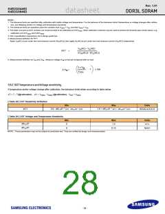
9.9 ODT Timing Definitions
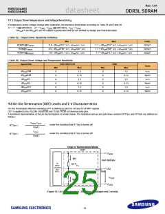
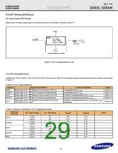
9.9.1 Test Load for ODT Timings
Different than for timing measurements, the reference load for ODT timings is defined in Figure 13.
VDDQ
DUT
DQ, DM
CK,CK
VTT
=
DQS , DQS
VSSQ
RTT
=25 ohm
TDQS , TDQS
VSSQ
Timing Reference Points
Figure 13. ODT Timing Reference Load
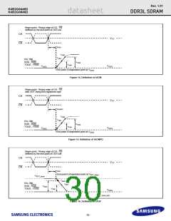
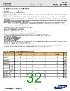
9.9.2 ODT Timing Definitions
Definitions for tAON, tAONPD, tAOF, tAOFPD and tADC are provided in Table 30 and subsequent figures. Measurement reference settings are provided
in Table 31 .
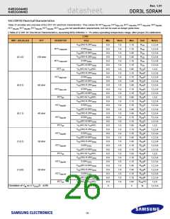
[ Table 30 ] ODT Timing Definitions
Symbol
tAON
Begin Point Definition
End Point Definition
Extrapolated point at VSSQ
Figure
Rising edge of CK - CK defined by the end point of ODTLon
Rising edge of CK - CK with ODT being first registered high
Rising edge of CK - CK defined by the end point of ODTLoff
Rising edge of CK - CK with ODT being first registered low
Figure 14
Figure 15
Figure 16
Figure 17
tAONPD
tAOF
Extrapolated point at VSSQ
End point: Extrapolated point at VRTT_Nom
End point: Extrapolated point at VRTT_Nom
tAOFPD
Rising edge of CK - CK defined by the end point of ODTLcnw,
ODTLcwn4 of ODTLcwn8
End point: Extrapolated point at VRTT_Wr and VRTT_Nom
respectively
tADC
Figure 18
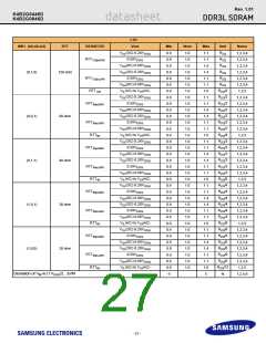
[ Table 31 ] Reference Settings for ODT Timing Measurements
Measured
RTT_Nom Setting
RTT_Wr Setting
VSW1[V]
VSW2[V]
NOTE
Parameter
RZQ/4
RZQ/12
RZQ/4
NA
NA
0.05
0.10
0.05
0.10
0.05
0.10
0.05
0.10
0.20
0.10
0.20
0.10
0.20
0.10
0.20
0.10
0.20
0.25
tAON
NA
tAONPD
tAOF
RZQ/12
RZQ/4
NA
NA
RZQ/12
RZQ/4
NA
NA
tAOFPD
tADC
RZQ/12
RZQ/12
NA
RZQ/2
- 29 -

 SAMSUNG [ SAMSUNG ]