Rev. 1.01
K4B2G0446D
K4B2G0846D
datasheet
DDR3L SDRAM
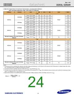
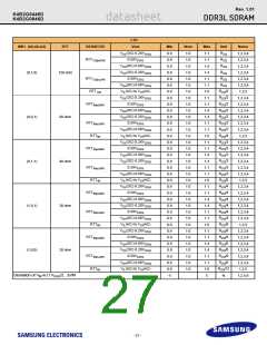
NOTE :
1. The tolerance limits are specified after calibration with stable voltage and temperature. For the behavior of the tolerance limits if temperature or voltage changes after calibra-
tion, see following section on voltage and temperature sensitivity
2. The tolerance limits are specified under the condition that V
= V and that V
= V
DDQ
DD
SSQ SS
3. Pull-down and pull-up ODT resistors are recommended to be calibrated at 0.5XV
. Other calibration schemes may be used to achieve the linearity spec shown above, e.g.
DDQ
calibration at 0.2XV
and 0.8XV
.
DDQ
DDQ
4. Not a specification requirement, but a design guide line
5. Measurement definition for RTT:
Apply V (AC) to pin under test and measure current I(V (AC)), then apply V (AC) to pin under test and measure current I(V (AC)) respectively
IH
IH
IL
IL
VIH(AC) - VIL(AC)
RTT
=
I(VIH(AC)) - I(VIL(AC))
6. Measurement definition for V and ∆V : Measure voltage (V ) at test pin (midpoint) with no load
M
M
M
2 x VM
VDDQ
- 1
x 100
∆ VM
=
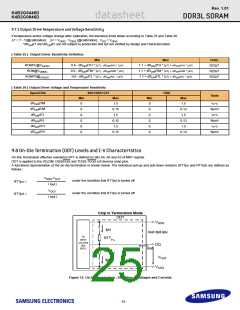
9.8.2 ODT Temperature and Voltage sensitivity
If temperature and/or voltage change after calibration, the tolerance limits widen according to table below
∆T = T - T(@calibration); ∆V = VDDQ - VDDQ (@calibration); VDD = VDDQ
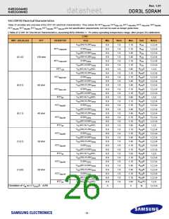
[ Table 28 ] ODT Sensitivity Definition
Min
Max
Units
0.9 - dRTTdT * |∆T| - dR dV * |∆V|
1.6 + dRTTdT * |∆T| + dR dV * |∆V|
RTT
RZQ/2,4,6,8,12
TT
TT
[ Table 29 ] ODT Voltage and Temperature Sensitivity
Min
0
Max
1.5
Units
%/°C
dRTTdT
dRTTdV
0
0.15
%/mV
NOTE : These parameters may not be subject to production test. They are verified by design and characterization.
- 28 -

 SAMSUNG [ SAMSUNG ]