Rev. 1.01
K4B2G0446D
K4B2G0846D
datasheet
DDR3L SDRAM
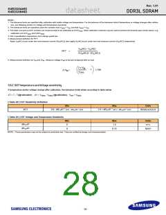
9.7.1 Output Drive Temperature and Voltage Sensitivity
If temperature and/or voltage change after calibration, the tolerance limits widen according to Table 25 and Table 26.
∆T = T - T(@calibration); ∆V = VDDQ - VDDQ (@calibration); VDD = VDDQ
*dRONdT and dRONdV are not subject to production test but are verified by design and characterization
[ Table 25 ] Output Driver Sensitivity Definition
Min
Max
Units
RONPU@VOHDC
RON@VOMDC
0.6 - dRONdTH * |∆T| - dR dVH * |∆V|
1.1 + dRONdTH * |∆T| + dR dVH * |∆V|
RZQ/7
RZQ/7
RZQ/7
ON
ON
0.9 - dRONdTM * |∆T| - dR dVM * |∆V|
1.1 + dRONdTM * |∆T| + dR dVM * |∆V|
ON
ON
RONPD@VOLDC
0.6 - dRONdTL * |∆T| - dR dVL * |∆V|
1.1 + dRONdTL * |∆T| + dR dVL * |∆V|
ON
ON
[ Table 26 ] Output Driver Voltage and Temperature Sensitivity
Speed Bin
800/1066/1333
1600
Units
Min
0
Max
1.5
Min
0
Max
1.5
dRONdTM
dRONdVM
dRONdTL
dRONdVL
dRONdTH
dRONdVH
%/°C
%/mV
%/°C
0
0.15
1.5
0
0.13
1.5
0
0
0
0.15
1.5
0
0.13
1.5
%/mV
%/°C
0
0
0
0.15
0
0.13
%/mV
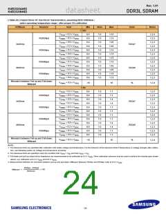
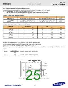
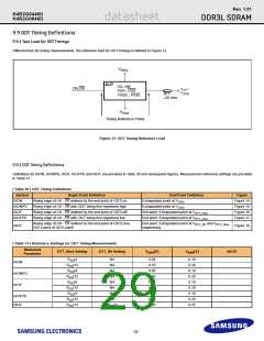
9.8 On-Die Termination (ODT) Levels and I-V Characteristics
On-Die Termination effective resistance RTT is defined by bits A9, A6 and A2 of MR1 register.
ODT is applied to the DQ,DM, DQS/DQS and TDQS,TDQS (x8 devices only) pins.
A functional representation of the on-die termination is shown below. The individual pull-up and pull-down resistors (RTTpu and RTTpd) are defined as
follows :
V
DDQ-VOUT
l Iout l
under the condition that RTTpd is turned off
under the condition that RTTpu is turned off
RTTpu =
RTTpd =
VOUT
l Iout l
Chip in Termination Mode
ODT
VDDQ
Ipu
Iout=Ipd-Ipu
To
RTTPu
other
circuitry
like
DQ
RCV,
Iout
RTTPd
...
VOUT
VSSQ
Ipd
Figure 12. On-Die Termination : Definition of Voltages and Currents
- 25 -

 SAMSUNG [ SAMSUNG ]