Rev. 1.01
K4B2G0446D
K4B2G0846D
datasheet
DDR3L SDRAM
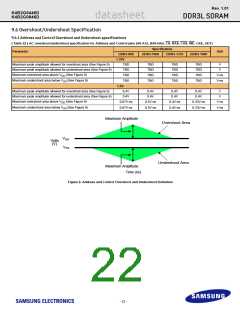
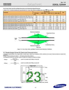
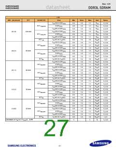
9.6.2 Clock, Data, Strobe and Mask Overshoot and Undershoot Specifications
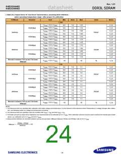
[ Table 23 ] AC overshoot/undershoot specification for Clock, Data, Strobe and Mask (DQ, DQS, DQS, DM, CK, CK)
Specification
Parameter
Unit
DDR3-800
1.35V
DDR3-1066
DDR3-1333
DDR3-1600
Maximum peak amplitude allowed for overshoot area (See Figure 10)
Maximum peak amplitude allowed for undershoot area (See Figure 10)
Maximum overshoot area above VDDQ (See Figure 10)
TBD
TBD
TBD
TBD
TBD
TBD
TBD
TBD
TBD
TBD
TBD
TBD
V
V
V-ns
Maximum undershoot area below VSSQ (See Figure 10)
TBD
TBD
TBD
TBD
V-ns
1.5V
Maximum peak amplitude allowed for overshoot area (See Figure 10)
Maximum peak amplitude allowed for undershoot area (See Figure 10)
Maximum overshoot area above VDDQ (See Figure 10)
0.4V
0.4V
0.4V
0.4V
0.4V
0.4V
0.4V
0.4V
V
V
0.25V-ns
0.25V-ns
0.19V-ns
0.15V-ns
0.13V-ns
V-ns
Maximum undershoot area below VSSQ (See Figure 10)
0.19V-ns
0.15V-ns
0.13V-ns
V-ns
Maximum Amplitude
Overshoot Area
VDDQ
VSSQ
Volts
(V)
Undershoot Area
Maximum Amplitude
Time (ns)
Figure 10. Clock, Data, Strobe and Mask Overshoot and Undershoot Definition
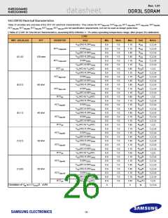
9.7 34ohm Output Driver DC Electrical Characteristics
A functional representation of the output buffer is shown below. Output driver impedance RON is defined by the value of external reference resistor RZQ
as follows:
RON34 = RZQ/7 (Nominal 34.3ohms +/- 10% with nominal RZQ=240ohm)
The individual Pull-up and Pull-down resistors (RONpu and RONpd) are defined as follows
VDDQ-VOUT
under the condition that RONpd is turned off
RONpu =
RONpd =
l Iout l
VOUT
l Iout l
under the condition that RONpu is turned off
Output Driver
VDDQ
Ipu
To
RON
other
Pu
circuity
DQ
Iout
RON
Pd
Vout
Ipd
VSSQ
Figure 11. Output Driver : Definition of Voltages and Currents
- 23 -

 SAMSUNG [ SAMSUNG ]