Rev. 1.01
K4B2G0446D
K4B2G0846D
datasheet
DDR3L SDRAM
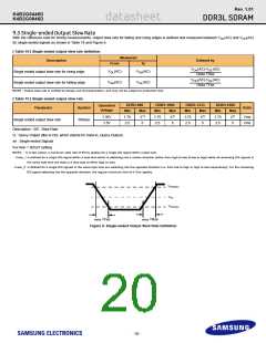
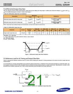
9.4 Differential Output Slew Rate
With the reference load for timing measurements, output slew rate for falling and rising edges is defined and measured between VOLdiff(AC) and VOH-
diff(AC) for differential signals as shown in Table 20 and Figure 7.
[ Table 20 ] Differential output slew rate definition
Measured
Description
Defined by
From
To
VOHdiff(AC)-VOLdiff(AC)
Delta TRdiff
VOLdiff(AC)
VOHdiff(AC)
Differential output slew rate for rising edge
Differential output slew rate for falling edge
VOHdiff(AC)-VOLdiff(AC)
Delta TFdiff
VOHdiff(AC)
VOLdiff(AC)
NOTE : Output slew rate is verified by design and characterization, and may not be subject to production test.
[ Table 21 ] Differential output slew rate
DDR3-800
DDR3-1066
DDR3-1333
DDR3-1600
Operation
Voltage
Parameter
Symbol
Units
Min
3.5
5
Max
12
Min
3.5
5
Max
12
Min
3.5
5
Max
12
Min
3.5
5
Max
12
1.35V
1.5V
V/ns
V/ns
Single ended output slew rate
Description : SR : Slew Rate
SRQdiff
10
10
10
10
Q : Query Output (like in DQ, which stands for Data-in, Query-Output)
diff : Differential Signals
For Ron = RZQ/7 setting
V
(AC)
OHdiff
V
V
TT
(AC)
OLdiff
delta TFdiff
delta TRdiff
Figure 7. Differential Output Slew Rate Definition
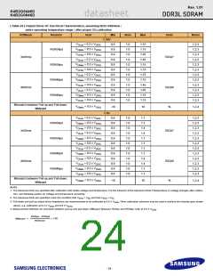
9.5 Reference Load for AC Timing and Output Slew Rate
Figure 8 represents the effective reference load of 25 ohms used in defining the relevant AC timing parameters of the device as well as output slew rate
measurements.
It is not intended as a precise representation of any particular system environment or a depiction of the actual load presented by a production tester. Sys-
tem designers should use IBIS or other simulation tools to correlate the timing reference load to a system environment. Manufacturers correlate to their
production test conditions, generally one or more coaxial transmission lines terminated at the tester electronics.
VDDQ
DQ
CK/CK
DQS
DUT
VTT = VDDQ/2
DQS
25Ω
Reference
Point
Figure 8. Reference Load for AC Timing and Output Slew Rate
- 21 -

 SAMSUNG [ SAMSUNG ]