PM9904BPD
ssaammeess
Commands
The demonstration software uses a buffer in memory on the
PC to generate the complete display. The buffer is dumped to
the LCD driver device in one go. The data passed to the driver
IC is formatted with a starting address followed by the data for
all segments. The first 8 bits is interpreted as address byte and
the rest of the data is sequentially passed as data bytes. The
address counter on the driver IC is incremented every 8
clocks. The procedure is repeated until all of the LCD memory
is filled up.
To write to the device the following address is passed:
1 0 A5 A4 A3 A2 A1 A0
Data
Data to the device is passed with MSB first
D7 D6 D5 D4 D3 D2 D1 D0
Were D7 and D3 map to pin VR[3] of driver and COM4 of LCD
Were D6 and D2 map to pin VR[2] of driver and COM3 of LCD
Were D5 and D1 map to pin VR[1] of driver and COM2 of LCD
Were D4 and D0 map to pin VR[0] of driver and COM1 of LCD
See SA8807A datasheet for more information.
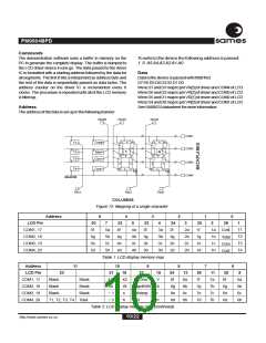
Address
The address of the data is set up in the following manner
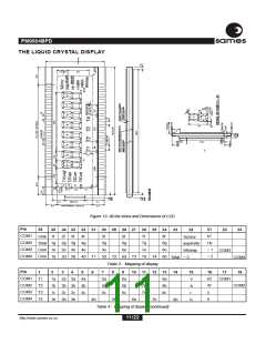
Pin36
Pin35
Pin32
COM1
a
a
Cosf
T1
f
b
f
b
COM2
1
4
T2
T3
Total
Com
g
g
COM3
COM4
e
c
e
c
T4
Cost
d
d
h
h
DR-01255
Pin1
Pin2
Pin5
COLUMNS
Figure 12: Mapping of a single character
Address
5
4
3
2
1
0
LCD Pin
COM1, 17
COM2, 18
COM3, 19
COM4, 20
30
5f
7
32
4f
5
33
3f
4
34
2f
3
35
1f
2
36
1
5a
5b
5c
5h
4a
4b
4c
4h
3a
3b
3c
3h
2a
2b
2c
2h
1a Cosi
T1
T2
T3
T4
5g
5e
5d
4g
4e
4d
3g
3e
3d
2g
2e
2d
1g
1e
1d
1b
1c
1h
Total
Com
Cost
Table 1: LCD display memory map
10
Address
LCD Pin
8
7
6
11
9
23
21
k1
16
k2
W
s
22
15
V
A
r
24
8f
13
26
7f
11
7a
7b
7c
7h
28
6f
9
COM1, 17
COM2, 18
COM3, 19
COM4, 20
Blank
Blank
Blank
Blank
Blank
Blank
% Error
imp/KWh
Wh/imp
~ 3
8a
8b
8c
8h
6a
6b
6c
6h
Hz
~ 1
~ 2
8g
8e
8d
7g
7e
7d
6g
6e
6d
T1, T2, T3, T4 Total
h
h
Table 2: LCD display memory map (continued)
10/22
http://www.sames.co.za

 SAMES [ SAMES ]