RU4099
Electrical Characteristics (TA=25°C Unless Otherwise Noted)
RU4099
Parameter
Test Condition
Unit
Min. Typ. Max.
Static Characteristics
BVDSS Drain-Source Breakdown Voltage
40
V
VGS=0V, IDS=250mA
VDS= 40V, VGS=0V
1
IDSS
Zero Gate Voltage Drain Current
mA
TJ=85°C
30
VGS(th) Gate Threshold Voltage
2
3
4
V
VDS=VGS, IDS=250mA
IGSS
Gate Leakage Current
VGS=±25V, VDS=0V
±100
3.5
nA
③
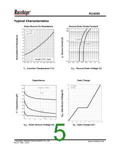
Drain-Source On-state Resistance VGS= 10V, IDS=40A
2.8
mW
RDS(ON)
Diode Characteristics
③
Diode Forward Voltage
ISD=40 A, VGS=0V
0.77
74
1.2
V
VSD
trr
Reverse Recovery Time
ns
nC
ISD=40A, dlSD/dt=100A/ms
qrr
Reverse Recovery Charge
148
④
Dynamic Characteristics
RG
Ciss
Coss
Crss
Gate Resistance
VGS=0V,VDS=0V,F=1MHz
1.4
5750
1400
480
21
W
Input Capacitance
VGS=0V,
VDS= 30V,
Frequency=1.0MHz
pF
Output Capacitance
Reverse Transfer Capacitance
td(ON) Turn-on Delay Time
tr Turn-on Rise Time
td(OFF) Turn-off Delay Time
tf Turn-off Fall Time
40
69
VDD=35V, RL=35W,
IDS= 1A, VGEN= 10V,
RG=6W
37
ns
75
136
208
115
④
Gate Charge Characteristics
Qg
Qgs
Qgd
Total Gate Charge
154
44
218
VDS=30V, VGS= 10V,
IDS=40A
nC
Gate-Source Charge
Gate-Drain Charge
47
Notes: ①Pulse width limited by safe operating area.
②Current limited by package( Limitation Current is 75A )
③Pulse test ; Pulse width£300ms, duty cycle£2%.
④Guaranteed by design, not subject to production testing.
2
CopyrightÓ Ruichips Semiconductor Co., Ltd
Rev.B –JUN., 2010
www.ruichips.com

 RUICHIPS [ RUICHIPS SEMICONDUCTOR CO., LTD ]