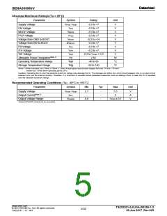
BD9A300MUV
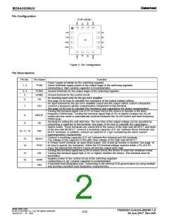
Pin Configuration
(TOP VIEW)
16
15
14
13
PVIN
PVIN
1
2
3
4
12 SW
11 SW
10 SW
FIN
PGND
PGND
9
SS
5
6
7
8
Figure 2. Pin Configuration
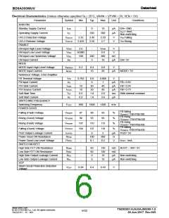
Pin Descriptions
Pin No.
1, 2
Pin Name
Function
Power supply terminals for the switching regulator.
These terminals supply power to the output stage of the switching regulator.
Connecting a 10µF ceramic capacitor is recommended.
PVIN
3, 4
5
PGND
AGND
Ground terminals for the output stage of the switching regulator.
Ground terminal for the control circuit.
An inverting input node for the gm error amplifier.
6
FB
See page 23 for how to calculate the resistance of the output voltage setting.
An input terminal for the gm error amplifier output and the output switch current comparator.
Connect a frequency phase compensation component to this terminal.
See page 24 for how to calculate the resistance and capacitance for phase compensation.
Turning this terminal signal Low (0.2V or lower) forces the device to operate in the fixed
frequency PWM mode. Turning this terminal signal High (0.8V or higher) enables the SLLM
control and the mode is automatically switched between the SLLM control and fixed frequency
PWM mode.
Terminal for setting the soft start time. The rise time of the output voltage can be specified by
connecting a capacitor to this terminal. See page 23 for how to calculate the capacitance.
Switch nodes. These terminals are connected to the source of the high-side MOSFET and drain
of the low-side MOSFET. Connect a bootstrap capacitor of 0.1µF between these terminals and
BOOT terminals. In addition, connect an inductor of 1.5µH considering the direct current
superimposition characteristic.
7
ITH
8
9
MODE
SS
10, 11, 12
SW
Connect a bootstrap capacitor of 0.1µF between this terminal and SW terminals.
The voltage of this capacitor is the gate drive voltage of the high-side MOSFET.
A “Power Good” terminal, an open drain output. Use of pull up resistor is needed. See page 18
for how to specify the resistance. When the FB terminal voltage reaches within ±7% of 0.8V
(Typ), the internal Nch MOSFET turns off and the output turns High.
13
14
BOOT
PGD
Turning this terminal signal low (0.8V or lower) forces the device to enter the shutdown mode.
Turning this terminal signal high (2.0V or higher) enables the device. This terminal must be
terminated.
15
EN
Supplies power to the control circuit of the switching regulator.
Connecting a 0.1µF ceramic capacitor is recommended.
A backside heat dissipation pad. Connecting to the internal PCB ground plane by using multiple
vias provides excellent heat dissipation characteristics.
16
-
AVIN
FIN
www.rohm.com
TSZ02201-0J3J0AJ00350-1-2
© 2013 ROHM Co., Ltd. All rights reserved.
2/32
30.Jun.2017 Rev.003
TSZ22111・15・001

 ROHM [ ROHM ]