Daattaasshheeeett
BD2041AFJ
BD2051AFJ
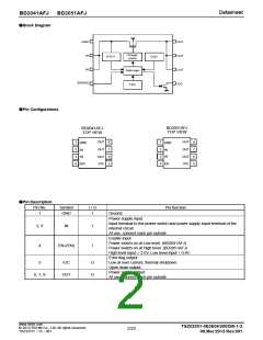
●Block Diagram
GND
OUT
OUT
OUT
/OC
Charge
pump
IN
UVLO
OCD
IN
Gate logic
TSD
EN(/EN)
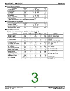
●Pin Configurations
BD2051AFJ
TOP VIEW
BD2041AFJ
TOP VIEW
OUT
OUT
1
2
3
4
8
7
6
5
1
2
3
4
8
7
6
5
GND
GND
OUT
OUT
IN
IN
IN
IN
OUT
/OC
OUT
/OC
EN
/EN
●Pin Description
Pin No.
1
Symbol
GND
I / O
I
Pin function
Ground.
Power supply input.
Input terminal to the power switch and power supply input terminal of the
internal circuit.
At use, connect each pin outside.
Enable input.
Power switch on at Low level. (BD2041AFJ)
Power switch on at High level. (BD2051AFJ)
High level input > 2.0V, Low level input < 0.8V.
Error flag output.
2, 3
4
IN
I
I
EN (/EN)
5
/OC
O
O
Low at over current, thermal shutdown.
Open drain output.
Power switch output.
6, 7, 8
OUT
At use, connect each pin outside.
www.rohm.com
© 2013 ROHM Co., Ltd. All rights reserved.
TSZ22111・15・001
TSZ02201-0E3E0H300290-1-2
2/22
08.Mar.2013 Rev.001

 ROHM [ ROHM ]