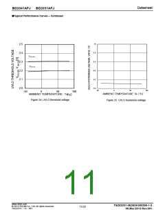
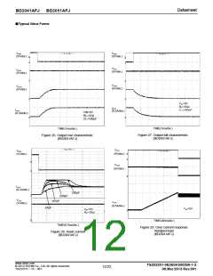
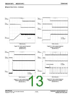
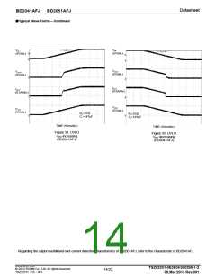
Daattaasshheeeett
BD2041AFJ
BD2051AFJ
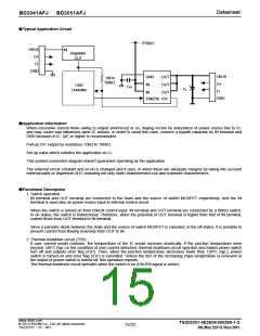
●Typical Application Circuit
5V(typ.)
VBUS
D+
IN
Regulator
OUT
D-
GND
VBUS
GND
IN
OUT
OUT
10k to
100kΩ
D+
USB
Controller
+
-
CIN
CL
D-
IN
OUT
/OC
GND
EN(/EN)
●Application Information
When excessive current flows owing to output shortcircuit or so, ringing occurs by inductance of power source line to IC,
and may cause bad influences upon IC actions. In order to avoid this case, connect a bypath capacitor by IN terminal and
GND terminal of IC. 1μF or higher is recommended.
Pull up /OC output by resistance 10kΩ to 100kΩ.
Set up value which satisfies the application as CL.
This system connection diagram doesn’t guarantee operating as the application.
The external circuit constant and so on is changed and it uses, in which there are adequate margins by taking into account
external parts or dispersion of IC including not only static characteristics but also transient characteristics.
●Functional Description
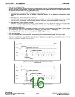
1. Switch operation
IN terminal and OUT terminal are connected to the drain and the source of switch MOSFET respectively. And the IN
terminal is used also as power source input to internal control circuit.
When the switch is turned on from EN/EN control input, IN terminal and OUT terminal are connected by a 80mΩ switch.
In on status, the switch is bidirectional. Therefore, when the potential of OUT terminal is higher than that of IN terminal,
current flows from OUT terminal to IN terminal.
Since a parasitic diode between the drain and the source of switch MOSFET is canceled, in the off status, it is possible to
prevent current from flowing reversely from OUT to IN.
2. Thermal shutdown circuit (TSD)
If over current would continue, the temperature of the IC would increase drastically. If the junction temperature were
beyond 140°C (typ.) in the condition of over current detection, thermal shutdown circuit operates and makes power switch
turn off and outputs error flag (/OC). Then, when the junction temperature decreases lower than 120°C (typ.), power
switch is turned on and error flag (/OC) is cancelled. Unless the fact of the increasing chips temperature is removed or
the output of power switch is turned off, this operation repeats.
The thermal shutdown circuit operates when the switch is on (EN,/EN signal is active).
www.rohm.com
© 2013 ROHM Co., Ltd. All rights reserved.
TSZ22111・15・001
TSZ02201-0E3E0H300290-1-2
08.Mar.2013 Rev.001
15/22

 ROHM [ ROHM ]