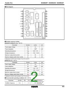
Audio ICs
BA6820F / BA6822S / BA6822F
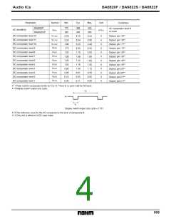
(2) LED drive outputs (pins 16 to 21)
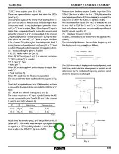
Release time: the time for pins 2 and 4 to go from 2V to
120mV (the level at which the first LED lights) when the
inputsignalgoesfroma1.8Vinputsignaltonosignal(the
input level at which the 12th LED lights is +6dB).
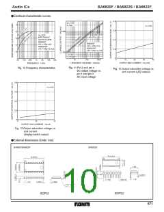
The recommended values are 10kΩ to 47kΩ for R1 and
R2 and 10µF to 22µF for C3 and C4. In DC mode, the at-
tack and release times are zero seconds regardless of
the RC circuits (see Fig. 7).
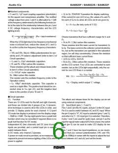
These are open-collector outputs that drive the LEDs
(see Fig. 5).
One complete cycle of the timing chart starting from O1
(pin 21) is as follows: if the channel 1 input is higher than
comparator level 1 during the first-point period for chan-
nel 1, a “L” level is output. Next, if the channel 1 input is
higher than comparator level 2 during the second-point
period for channel 1, a “L” level is output, if the channel
2 input is higher than comparator level 1 during the first-
point period for channel 2, a “L” level is output, and then
if the channel 2 input is higher than comparator level 2
during the second-point period for channel 2, a “L” level
is output.This cycle is then repeated for outputs O2 to O6.
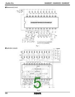
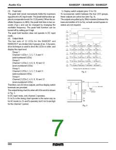
(5) Mode switch pins (pins 6, 7 and 8)
S AC/DC mode switch pin (pin 6)
(7) Oscillator frequency (pin 9)
R3 and C5 connected to pin 9 determine the oscillator fre-
quency.
The relationship between the oscillator frequency and
the display switching period is as follows:
When “H” AC input (pins 1 and 3) is selected, and when
“L” DC input (pin 5) is selected.
“H”: 1, 3pin “L”: 5pin
S Mute (pin 7)
The LED drive output, display switch output period, peak
hold time, and mute time when power is applied are all
determined by the oscillation frequency, and are varied
when the frequency is changed.
When “H”, mute is applied, and no display is output. Nor-
mally “L”.
S Peak hold (pin 8)
When “H”, peak hold for AC input is cancelled.
The circuit for these three mode switches is given in Fig.
6.
Pins 6 to 8 are pulled down by a 50kΩ resistor, so there
is no need for the inputs to be connected to GND for a “L”
input.
(6) Attack and release times (pins 2 and 4)
The output response to AC input signals is set by the RC
circuits connected to pins 2 and 4 (R1 and C3 for channel
1, and R2 and C4 for channel 2).
Attack time: the time for pins 2 and 4 to go from 0V to 2V
(whenall 12 LEDs are lit) when the input signal goes from
no signal to a 1.8V input signal with f = 1kHz (the input
level at which the 12th LED lights is +6dB).
669

 ROHM [ ROHM ]