Audio ICs
BA5415A / BA5416
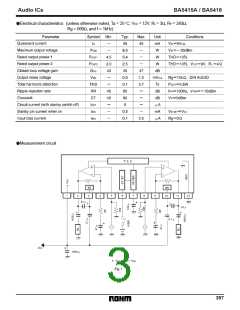
FOperation notes
(1) Input circuit
(3) Oscillation countermeasures
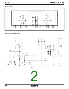
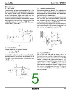
The structure of the input circuit is shown in Fig. 4. The
IC can be used without coupling capacitors, but a maxi-
mum of 0.5µA of bias current (IBIN) flows from the input
pin, so if potentiometer sliding noise results from this,
connect an input capacitor CIN as shown below.
To prevent degradation of the IC characteristics, the input
bias resistor is not built into the IC. Connect an input bias
resistor (RIN) between the input and GND (the recom-
mended value is about 33kΩ).
We recommend that the capacitor (C1) connected be-
tween the B. S pin and the VCC pin for oscillation preven-
tion be a metal-film component with good temperature
and high-frequency characteristics.
Ceramic capacitors have poor temperature characteris-
tics, so if used, allow sufficient oscillation margin. It is
also possible to connect a capacitor for oscillation pre-
vention between the output and GND (C2).
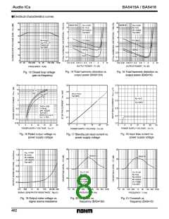
The oscillation margin depends on the PCB pattern and
the mounting position of the capacitor. Design your PCB
after referring to the application example PCB.
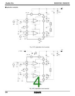
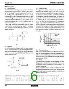
(2) Gain adjustment
The gain is given by the following formula.
RNF)RF
GV = 20log
RF
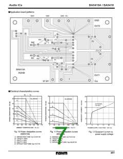
(4) VCC and GND lines
The Pre. GND and Pow. GND are joined at pin 12, so
there is a chance of crosstalk or degraded distortion per-
formance due to common ground impedance in the PCB
pattern. In addition, the power supply capacitor con-
nected between VCC and GND is influenced by the PCB
pattern, and common VCC and GND impedance may de-
grade the ripple rejection and distortion. Design the PCB
after referring to the application example PCB (the rec-
ommended value for the power supply capacitor is
1000µF of greater).
It is possible to reduce the gain by increasing RF, but the
amount of feedback will increase, and oscillation will be
more likely to occur. We recommend that you set the gain
to 30dB or higher.
399

 ROHM [ ROHM ]