BA10358xx, BA10324Axx, BA2904xxx, BA2904Sxxx, BA2904Wxx
BA2902xx, BA2902Sxx
Datasheet
VCC
●Operational Notes
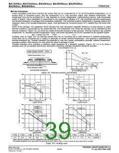
1) Unused circuits
+
-
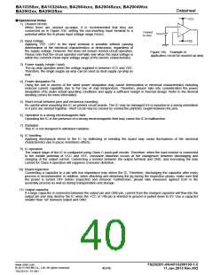
When there are unused op-amps, it is recommended that they are
connected as in Figure 104, setting the non-inverting input terminal to a
potential within the in-phase input voltage range (Vicm).
Connect
to Vicm
Vicm
2) Input voltage
VEE
Applying VEE +32V to the input terminal is possible without causing
deterioration of the electrical characteristics or destruction, regardless of
the supply voltage. However, this does not ensure normal circuit operation.
Please note that the circuit operates normally only when the input voltage is
within the common mode input voltage range of the electric characteristics.
Figure 104. Example of
application circuit for unused op-amp
3) Power supply (single / dual)
The op-amp operates when the voltage supplied is between VCC and VEE.
Therefore, the single supply op-amp can be used as dual supply op-amp as
well.
4) Power dissipation Pd
Using the unit in excess of the rated power dissipation may cause deterioration in electrical characteristics including
reduced current capability due to the rise of chip temperature. Therefore, please take into consideration the power
dissipation (Pd) under actual operating conditions and apply a sufficient margin in thermal design. Refer to the thermal
derating curves for more information.
5) Short-circuit between pins and erroneous mounting
Be careful when mounting the IC on printed circuit boards. The IC may be damaged if it is mounted in a wrong orientation
or if pins are shorted together. Short circuit may be caused by conductive particles caught between the pins.
6) Operation in a strong electromagnetic field
Operating the IC in the presence of a strong electromagnetic field may cause the IC to malfunction.
7) Radiation
This IC is not designed to withstand radiation.
8) IC handling
Applying mechanical stress to the IC by deflecting or bending the board may cause fluctuations of the electrical
characteristics due to piezo resistance effects.
9) IC operation
The output stage of the IC is configured using Class C push-pull circuits. Therefore, when the load resistor is connected
to the middle potential of VCC and VEE, crossover distortion occurs at the changeover between discharging and
charging of the output current. Connecting a resistor between the output terminal and GND, and increasing the bias
current for Class A operation will suppress crossover distortion.
10) Board inspection
Connecting a capacitor to a pin with low impedance may stress the IC. Therefore, discharging the capacitor after every
process is recommended. In addition, when attaching and detaching the jig during the inspection phase, make sure that
the power is turned OFF before inspection and removal. Furthermore, please take measures against ESD in the
assembly process as well as during transportation and storage.
11) Output capacitor
If a large capacitor is connected between the output pin and GND pin, current from the charged capacitor will flow into the
output pin and may destroy the IC when the VCC or VIN pin is shorted to ground or pulled down to 0V. Use a capacitor
smaller than 1uF between output and GND.
www.rohm.com
© 2013 ROHM Co., Ltd. All rights reserved.
TSZ22111・15・001
TSZ02201-0RAR1G200130-1-2
11.Jan.2013 Rev.002
40/45

 ROHM [ ROHM ]