ꢀ
ꢀ ꢀ ꢀ ꢀ ꢀ ꢀ ꢀ ꢀ
2SAR562F3
ꢀ ꢀ ꢀ ꢀꢀ
Datasheet
llAbsolute maximum ratings (Ta = 25°C)
Parameter
Symbol
VCBO
VCEO
VEBO
IC
Values
Unit
V
V
V
A
Collector-base voltage
Collector-emitter voltage
Emitter-base voltage
-30
-30
-6
-6
-7
Collector current
Power dissipation
*1
ICP
A
*2
PD
1.0
2.1
W
W
℃
℃
*3
PD
Tj
Tstg
Junction temperature
Range of storage temperature
150
-55 to +150
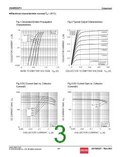
llElectrical characteristics (Ta = 25°C)
Values
Typ.
Parameter
Symbol
Conditions
Unit
Min.
-30
Max.
-
Collector-base breakdown
voltage
Collector-emitter breakdown
voltage
BVCBO
BVCEO
I = -100μA
-
V
V
C
I = -1mA
-30
-
-
C
BVEBO
ICBO
I = -100μA
Emitter-base breakdown voltage
Collector cut-off current
-6
-
-
V
nA
nA
mV
-
E
V
CB
= -30V
-
-
-100
-100
-300
500
IEBO
V = -4V
EB
Emitter cut-off current
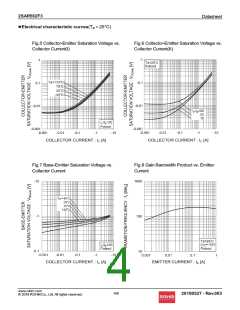
Collector-emitter saturation voltage
-
-
-
-150
-
V
I = -3A, I = -150mA
CE(sat)
C
B
hFE
V
CE
= -2V, I = -500mA
DC current gain
200
C
V
= -10V, I = 200mA,
E
CE
f
Transition frequency
-
-
-
-
-
180
75
-
-
-
-
-
MHz
pF
ns
T
f = 100MHz
V
CB
= -10V, I = 0A,
E
Cob
ton
tstg
tf
Output capacitance
Turn-On time
Storage time
Fall time
f = 1MHz
I = 3A,
C
25
I = 300mA,
B1
I = -300mA,
B2
150
40
ns
V
CC
⋍ 10V,
R = 3.3Ω
See test circuit
L
ns
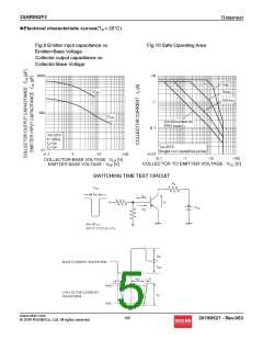
ꢀ ꢀ ꢀ ꢀ ꢀ ꢀ ꢀ ꢀ ꢀ ꢀ ꢀ ꢀ ꢀꢀ ꢀ ꢀ ꢀꢀꢀ ꢀ ꢀ ꢀ
ꢀꢀ ꢀ ꢀ ꢀꢀꢀ ꢀ ꢀ ꢀ ꢀ ꢀ ꢀ ꢀ ꢀ ꢀ ꢀ
*1ꢀPw=1ms Single Pulse
2
*2ꢀMounted on FR4 board(25.4×25.4×1.6mm, Cu PAD:645mm ).
*3ꢀPw=10ms
2
ꢀꢀMounted on FR4 board(25.4×25.4×1.6mm, Cu PAD:645mm ).
ꢀ ꢀ ꢀ ꢀ ꢀ ꢀ ꢀ ꢀ ꢀ ꢀ ꢀ ꢀ ꢀ ꢀ ꢀ ꢀ ꢀ ꢀ ꢀꢀ ꢀ ꢀ ꢀ
ꢀ
ꢀꢀ ꢀ ꢀ ꢀꢀꢀ ꢀ ꢀ ꢀ ꢀ ꢀ ꢀ ꢀ ꢀ ꢀ ꢀ ꢀ ꢀ ꢀ ꢀ ꢀ
www.rohm.com
© 2019 ROHMCo., Ltd. All rights reserved.
2/6
20190527 - Rev.003

 ROHM [ ROHM ]