OP1177/OP2177/OP4177
TABLE OF CONTENTS
Features .............................................................................................. 1
Overload Recovery Time .......................................................... 15
THD + Noise............................................................................... 16
Capacitive Load Drive ............................................................... 16
Stray Input Capacitance Compensation.................................. 17
Reducing Electromagnetic Interference.................................. 17
Proper Board Layout.................................................................. 18
Difference Amplifiers ................................................................ 18
A High Accuracy Thermocouple Amplifier........................... 19
Low Power Linearized RTD...................................................... 19
Single Operational Amplifier Bridge....................................... 20
Realization of Active Filters .......................................................... 21
Band-Pass KRC or Sallen-Key Filter........................................ 21
Channel Separation.................................................................... 21
References on Noise Dynamics and Flicker Noise ............... 21
Outline Dimensions....................................................................... 22
Ordering Guide .......................................................................... 24
Applications....................................................................................... 1
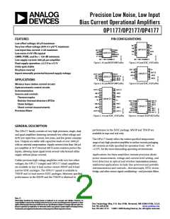
Pin Configurations ........................................................................... 1
General Description......................................................................... 1
Revision History ............................................................................... 2
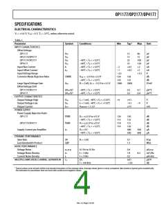
Specifications..................................................................................... 3
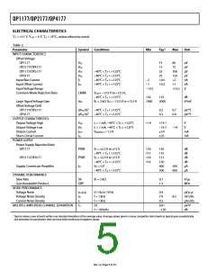
Electrical Characteristics............................................................. 4
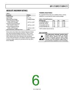
Absolute Maximum Ratings............................................................ 5
Thermal Resistance ...................................................................... 5
ESD Caution.................................................................................. 5
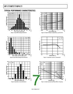
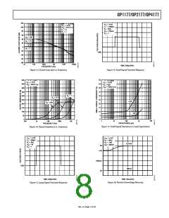
Typical Performance Characteristics ............................................. 6
Functional Description.................................................................. 14
Total Noise-Including Source Resistors................................... 14
Gain Linearity ............................................................................. 14
Input Overvoltage Protection ................................................... 15
Output Phase Reversal............................................................... 15
Settling Time............................................................................... 15
REVISION HISTORY
Changes to Figure 67 and Figure 68............................................. 21
Removed SPICE Model Section ................................................... 21
Updated Outline Dimensions....................................................... 22
Changes to Ordering Guide.......................................................... 24
11/09—Rev. F to Rev. G
Changes to Figure 64...................................................................... 19
Changes to Ordering Guide .......................................................... 24
Updated Outline Dimensions....................................................... 22
4/04—Rev. B to Rev. C
5/09—Rev. E to Rev. F
Changes to Ordering Guide.............................................................4
Changes to TPC 6..............................................................................5
Changes to TPC 26............................................................................7
Updated Outline Dimensions....................................................... 17
Changes to Figure 64...................................................................... 19
Changes to Ordering Guide .......................................................... 24
10/07—Rev. D to Rev. E
Changes to General Description .................................................... 1
Changes to Table 4............................................................................ 5
Updated Outline Dimensions....................................................... 22
4/02—Rev. A to Rev. B
Added OP4177.........................................................................Global
Edits to Specifications.......................................................................2
Edits to Electrical Characteristics Headings..................................4
Edits to Ordering Guide ...................................................................4
7/06—Rev. C to Rev. D
Changes to Table 4............................................................................ 5
Changes to Figure 51...................................................................... 14
Changes to Figure 52...................................................................... 15
Changes to Figure 54...................................................................... 16
Changes to Figure 58 to Figure 61................................................ 17
Changes to Figure 62 and Figure 63............................................. 18
Changes to Figure 64...................................................................... 19
Changes to Figure 65 and Figure 66............................................. 20
11/01—Rev. 0 to Rev. A
Edit to Features ..................................................................................1
Edits to TPC 6 ...................................................................................5
7/01—Revision 0: Initial Version
Rev. G | Page 2 of 24

 ROCHESTER [ Rochester Electronics ]