AD8510/AD8512/AD8513
ABSOLUTE MAXIMUM RATINGS
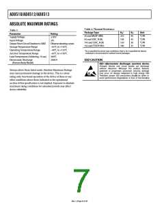
Table 3.
Table 4. Thermal Resistance
Package Type
1
θJA
θJC
45
43
36
35
Unit
°C/W
°C/W
°C/W
°C/W
Parameter
Rating
8-Lead MSOP (RM)
8-Lead SOIC_N (R)
14-Lead SOIC_N (R)
14-Lead TSSOP (RU)
210
158
120
180
Supply Voltage
18 V
Input Voltage
VS
Output Short-Circuit Duration to GND
Storage Temperature Range
Operating Temperature Range
Junction Temperature Range
Lead Temperature (Soldering, 10 sec)
Observe derating curves
−65°C to +150°C
−40°C to +125°C
−65°C to +150°C
300°C
1 θJA is specified for worst-case conditions, that is, θJA is specified for device
soldered in circuit board for surface-mount packages.
Electrostatic Discharge
(Human Body Model)
2000 V
ESD CAUTION
Stresses above those listed under Absolute Maximum Ratings
may cause permanent damage to the device. This is a stress
rating only; functional operation of the device at these or any
other conditions above those indicated in the operational
section of this specification is not implied. Exposure to absolute
maximum rating conditions for extended periods may affect
device reliability.
Rev. I | Page 6 of 20

 ROCHESTER [ Rochester Electronics ]