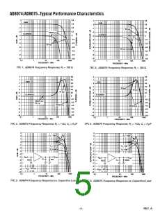
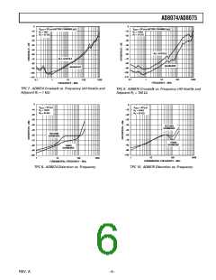
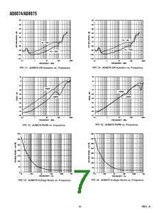
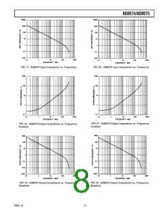
AD8074/AD8075
ORDERING GUIDE
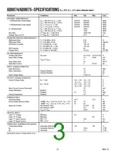
ABSOLUTE MAXIMUM RATINGS1
Supply Voltage . . . . . . . . . . . . . . . . . . . . . . . . . . . . . . . . . 12.0 V
Temperature
Range
Package
Description
Package
Option
Internal Power Dissipation2, 3
Model
AD8074/AD8075 16-Lead TSSOP (RU) . . . . . . . . . . . . . 1 W
Input Voltage
AD8074ARU
AD8075ARU
AD8074-EVAL
AD8075-EVAL
–40°C to +85°C 16-Lead Plastic TSSOP RU-16
–40°C to +85°C 16-Lead Plastic TSSOP RU-16
Evaluation Board
IN0, IN1, IN2 . . . . . . . . . . . . . . . . . . . . . . . . . VEE ≤ VIN ≤ VCC
OE . . . . . . . . . . . . . . . . . . . . . . . . . . . . . DGND ≤ VIN ≤ VCC
Output Short Circuit Duration . . . . . . . . . . . . . . . . . . Indefinite3
Storage Temperature Range . . . . . . . . . . . . . . –65°C to +150°C
Lead Temperature Range (Soldering 10 sec) . . . . . . . . . . . 300°C
Evaluation Board
PIN CONFIGURATION
NOTES
1Stresses above those listed under Absolute Maximum Ratings may cause perma-
nent damage to the device. This is a stress rating only; functional operation of the
device at these or any other conditions above those indicated in the operational
section of this specification is not implied. Exposure to absolute maximum rating
conditions for extended periods may affect device reliability.
2Specification is for device in free air (TA = 25°C).
AD8074/AD8075
1
2
3
4
5
6
7
8
16
15
V
CC
OE
DGND
IN2
V
CC
G =
14 OUT2
13
+1/+2
316-lead plastic TSSOP; θJA = 150.4°C/W. Maximum internal power dissipa-
V
AGND
IN1
EE
12 OUT1
11
tion (PD
) should be derated for ambient temperature (TA) such that
PD < (150°C – TA)/θJA
.
G =
+1/+2
V
AGND
IN0
CC
G =
+1/+2
10 OUT0
V
V
9
EE
EE
CAUTION
ESD (electrostatic discharge) sensitive device. Electrostatic charges as high as 4000 V readily
accumulate on the human body and test equipment and can discharge without detection. Although
the AD8074/AD8075 features proprietary ESD protection circuitry, permanent damage may occur
on devices subjected to high-energy electrostatic discharges. Therefore, proper ESD precautions
are recommended to avoid performance degradation or loss of functionality.
WARNING!
ESD SENSITIVE DEVICE
1.5
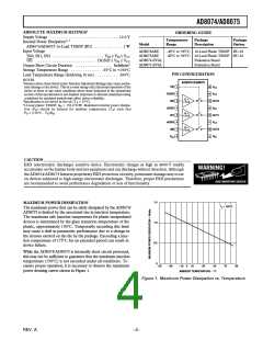
MAXIMUM POWER DISSIPATION
T
= 150؇C
J
The maximum power that can be safely dissipated by the AD8074/
AD8075 is limited by the associated rise in junction temperature.
The maximum safe junction temperature for plastic encapsulated
devices is determined by the glass transition temperature of the
1.0
plastic, approximately 150°C. Temporarily exceeding this limit
may cause a shift in parametric performance due to a change in
the stresses exerted on the die by the package. Exceeding a junc-
tion temperature of 175°C for an extended period can result in
device failure.
0.5
While the AD8074/AD8075 is internally short circuit protected,
this may not be sufficient to guarantee that the maximum junction
temperature (150°C) is not exceeded under all conditions. To
ensure proper operation, it is necessary to observe the maximum
power derating curves shown in Figure 1.
0
–50
–30
–10
0
10
30
50
90
70
AMBIENTTEMPERATURE – ؇C
Figure 1. Maximum Power Dissipation vs. Temperature
REV. A
–3–

 ROCHESTER [ Rochester Electronics ]