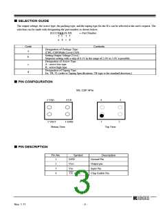
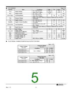
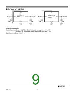
■ SELECTION GUIDE
The output voltage, the active type, the packing type, and the taping type for the ICs can be selected at the user's request. The
selection can be made with designating the part number as shown below;
R1113XXX1X-XX
←Part Number
↑ ↑ ↑ ↑
a
b c d
Code
Contents
Designation of Package Type :
Z:WL-CSP(Wafer Level CSP)
Setting Output Voltage (VOUT) :
a
b
c
d
Stepwise setting with a step of 0.1V in the range of 2.0V to 5.0V is possible.
Designation of Active Type :
A : active low type
B : active high type
Designation of Taping Type :
Ex. TR, TL (refer to Taping Specifications; TR type is the standard direction.)
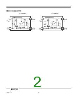
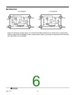
■ PIN CONFIGURATION
WL-CSP 4Pin
4
3
3 VDD
4 CE
1
2
2 VOUT
1 GND
Top View
Botom View
■ PIN DESCRIPTION
Pin No.
Symbol
GND
Description
1
Ground Pin
2
3
4
VOUT
VDD
CE
Output pin
Input Pin
or CE
Chip Enable Pin
Rev. 1.11
- 3 -

 RICOH [ RICOH ELECTRONICS DEVICES DIVISION ]