RT9701
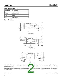
Pin Description
Pin Name
VIN
Pin Function
Power Input
Output Voltage
Ground
VOUT
GND
CE
Chip Enable
Test Circuits
VOUT
VIN
IOUT
RT9701 CBL
VIN
VOUT
VIN
VOUT
+
+
IL
GND
RL
CIN
CL
Test Circuit 1
VOUT
VIN
VIN-SW
RT9701 CBL
VIN
VOUT
Switch Off
VIN
VOUT
+
+
GND
RL
CL
CIN
Test Circuit 2
VOUT
VIN
IOUT
RT9701 CB
VIN
CE
VOUT
VOUT
GND
VCE
+
+
IL
RL
CIN
CL
On
Off
Test Circuit 3
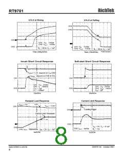
Test Circuit 2 is performed by charging an external tank of bulk capacitor to the input then applying this voltage to
the input of the unit.
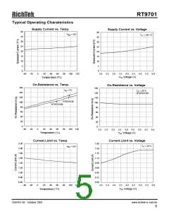
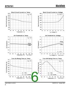
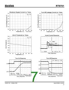
All typical operating characteristics curves showed are referred to Test Circuit 1, unless specified to Test Circuit 2
or Test Circuit 3.
www.richtek-ic.com.tw
DS9701-05 October 2001
2

 RICHTEK [ RICHTEK TECHNOLOGY CORPORATION ]